
Backlight unit and liquid crystal display device including the same

A backlight unit and device technology, applied in the direction of semiconductor devices, optical components, electrical components, etc.

Inactive Publication Date: 2016-05-25
LG DISPLAY CO LTD
View PDF9 Cites 4 Cited by
  • Summary
  • Abstract
  • Description
  • Claims
  • Application Information

AI Technical Summary

Problems solved by technology

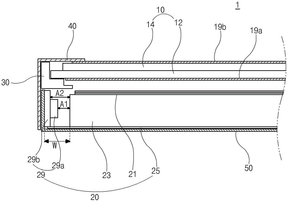
However, since the LED assembly 29 needs to be separated from the light guide plate 23 by a certain distance, it is difficult to reduce the width W of the bezel area, which is equivalent to the first gap distance A1 in the LCD device 1, the thickness of each LED 29a, and the thickness of the LEDPCB 29b. sum of thickness

Method used


Image

  • Backlight unit and liquid crystal display device including the same
  • Backlight unit and liquid crystal display device including the same
  • Backlight unit and liquid crystal display device including the same

Examples


Embodiment approach

[0050] exist Figure 6 In this case, the leads 298 of the plurality of LEDs 290 do not protrude beyond the lower surface of the LEDPCB 280 . Similar to the first embodiment of the present invention, the LEDPCB 280 includes a base layer 281 , an insulating layer 282 on the base layer 281 , a circuit pattern layer 283 on the insulating layer 282 , and a protection layer 284 on the circuit pattern layer 283 . In addition, a plurality of through holes 288 are formed in the LEDPCB 280 along the long sides of the LEDPCB 280 . The lead groove 286 surrounding each of the plurality of through holes 288 is formed such that the base layer 281, the insulating layer 282, and the circuit pattern layer 283 each have a step difference.

[0051] The LED assembly 200 includes an LEDPCB 280 and a plurality of light emitting diodes 290 inserted into a plurality of through holes 288 of the LEDPCB 280 . The base layer 281 may include a metal material having relatively high thermal conductivity su...


PUM


Abstract

The invention relates to a light emitting diode assembly, a backlight unit including the light-emitting diode component and a liquid crystal display device. The light emitting diode assembly includes: a light emitting diode (LED) printed circuit board (PCB) and a plurality of LEDs. The PCB has a base layer, an insulating layer,a circuit pattern layer and a protection layer from top to bottom, wherein LED PCB includes a plurality of through holes spaced apart from each other along a long side direction; and a plurality of light emitting diodes (LEDs) are inserted into the plurality of through holes, respectively, from a bottom surface of the LED PCB, wherein the LEDs comprise leads on two sides of the LEDs, and are in electric connection with the LED PCB through the leads.

Description

[0001] This application is a divisional application of Chinese patent application 201110439014.X. technical field [0002] The invention relates to a liquid crystal display device. More particularly, the present invention relates to a liquid crystal display device having a narrow bezel area due to a light emitting diode (LED) backlight unit. Background technique [0003] Liquid crystal display (LCD) devices utilize the optical anisotropy and polarization properties of liquid crystal molecules, and are superior in displaying moving images and high-contrast images, and are currently widely used in televisions or monitors. A liquid crystal display device includes a liquid crystal panel composed of two substrates facing each other and a liquid crystal layer between the substrates. The alignment direction of the liquid crystal molecules in the liquid crystal panel will change with the electric field, so the liquid crystal panel will have a difference in light transmittance. [...

Claims


Application Information

Patent Timeline
Patent Type & Authority Applications(China)
IPC IPC(8): G02F1/13357H05K1/18
CPCG02F1/133615H05K1/183H05K2201/10106G02B6/0083G02B6/0093F21Y2103/10F21Y2115/10G02B6/0091G02F1/1336G02F1/133603H01L33/48G02F1/13332G02F1/133314F21V19/0025G02B6/0051G02B6/0073G02F1/133308
Inventor 权宁敏闵志殒千昊永
Owner LG DISPLAY CO LTD
Learn More