Semiconductor components with weak current paths

A weak current, semiconductor technology, used in semiconductor devices, electrical components, circuits, etc., can solve the problems of reduction, energy consumption operation accuracy, and high on-resistance

Inactive Publication Date: 2019-01-29
RICHTEK TECH
View PDF3 Cites 0 Cited by
  • Summary
  • Abstract
  • Description
  • Claims
  • Application Information

AI Technical Summary

Problems solved by technology

However, when the control voltage of the gate G is in the weak voltage (low voltage) range, the on-resistance is relatively high, and operation errors are prone to occur at weak voltages, such as conduction when it should be turned on but cannot be turned on
Therefore, although the design of the semiconductor device 10 may have better high-voltage operation characteristics, it will cause unnecessary energy consumption and lower operation accuracy in the weak voltage range.

Method used


Image

  • Semiconductor components with weak current paths
  • Semiconductor components with weak current paths
  • Semiconductor components with weak current paths

Examples


Embodiment Construction

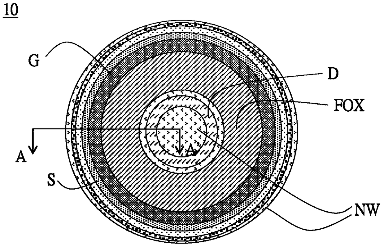
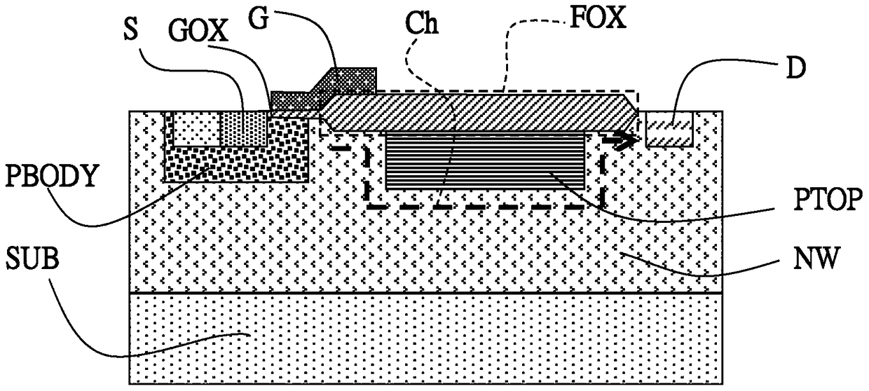
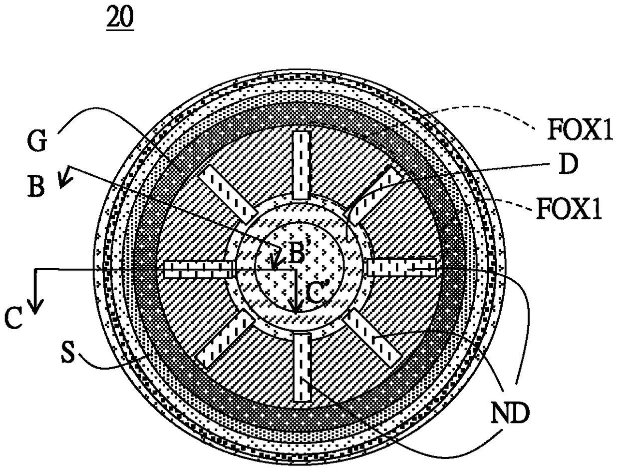
[0036] The foregoing and other technical contents, features and effects of the present invention will be clearly presented in the following detailed description of a preferred embodiment with reference to the drawings. The drawings in the present invention are schematic and mainly intended to show the relative positional relationship between the various regions, and the shapes, thicknesses and widths are not drawn to scale.

[0037] Figures 2A-2C It is shown that the present invention provides a semiconductor element 20, wherein Figure 2A for top view, Figure 2B based on Figure 2A Sectional view of cutting line BB', Figure 2C based on Figure 2A Sectional view of cutting line CC'. and Figures 1A-1B Compared with the prior art, the main difference is that the insulating layer FOX of the semiconductor element 10 in the prior art is a continuous structure, and the first conductive type lightly doped regions ND are respectively provided between the insulating layers FOX...


PUM


Abstract

The invention provides a semiconductor component possessing a low current pathway. The semiconductor component possesses a grid, a source electrode and a drain electrode. A plurality of insulating layers and a plurality of first conductive-type shallow doped areas are arranged between the grid and the drain electrode and are arranged in a staggered mode. The plurality of first conductive-type shallow doped areas provide a low current pathway between the source electrode and the drain electrode. When the grid is in a relative low voltage scope, the low current pathway is conducted. When the grid is in a relative high voltage scope, the low current pathway is not conducted.

Description

technical field [0001] The invention relates to a semiconductor element, especially a semiconductor element in which a shallow doped region of the first conductivity type can provide a weak current path when the gate is in a weak voltage range. Background technique [0002] Figures 1A-1B The shown existing semiconductor element 10 has the structure of a field effect transistor with double surface electric field reduction (Double Resurf), wherein Figure 1B based on Figure 1A Sectional view of the cutting line AA'. The semiconductor element 10 includes a substrate SUB on which a first conductivity type well NW is disposed, and the first conductivity type well NW is formed from Figure 1B From left to right, there are respectively a second conductivity type body region PBODY, a source S, an insulating layer FOX, and a drain D, and a second conductivity type well region PTOP is located under the insulating layer FOX. The semiconductor device 10 further includes a gate G di...

Claims


Application Information

Patent Timeline
Patent Type & Authority Patents(China)
IPC IPC(8): H01L29/06H01L29/36H01L29/78
Inventor 黄宗义邱建维朱焕平张建凯
Owner RICHTEK TECH
Why Eureka
Try Eureka