P-i-n juncture photovoltaic device in molecules of carbon nano tube based on local district doping and preparation method
A p-i-n, carbon nanotube technology, used in photovoltaic power generation, semiconductor devices, electrical components, etc., can solve the problem that asymmetric structure cannot well achieve photovoltaic performance regulation, can not fully exert the excellent performance of carbon nanotubes, and increase contact resistance. and other problems, to achieve the effect of excellent photovoltaic performance, maintaining integrity and stable performance
- Summary
- Abstract
- Description
- Claims
- Application Information
AI Technical Summary
Problems solved by technology
Method used
Image

Examples
Embodiment 1
[0034] This embodiment includes the following steps:
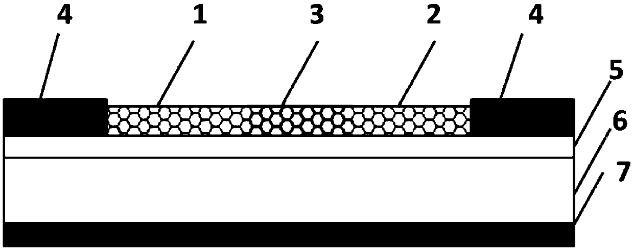
[0035] In the first step, the ultrasonically dispersed carbon nanotube solution is spin-coated on the surface of the substrate. After the solvent is completely evaporated, the substrate is observed with a scanning electron microscope and the carbon nanotubes with a length of 5 μm are selected, and the carbon nanotubes are positioned with the aid of the prefabricated cross mark on the substrate.
[0036] In the second step, electron beam lithography and magnetron sputtering techniques are used to fabricate Au symmetrical electrodes at both ends of the carbon nanotubes, with an electrode spacing of 3 μm.
[0037] In the third step, electron beam photoresist is coated on the substrate, and one end of the carbon nanotube is exposed to a window by electron beam lithography technology, and the window size is 1 μm*1 μm. The exposed portion (1 μm) of the carbon nanotubes will be exposed to air after being developed and fixed. Th...
Embodiment 2
[0042] This embodiment includes the following steps:
[0043] In the first step, the ultrasonically dispersed carbon nanotube solution is coated on the surface of the substrate. After the solvent is completely evaporated, the substrate is observed with a scanning electron microscope and the carbon nanotubes with a length of more than 6 μm are selected, and the carbon nanotubes are positioned with the aid of the pre-fabricated cross marks on the substrate.
[0044] In the second step, electron beam lithography and magnetron sputtering techniques are used to fabricate Au symmetrical electrodes at both ends of the carbon nanotubes, with an electrode spacing of 4 μm.
[0045] In the third step, electron beam photoresist is coated on the substrate, and one end of the carbon nanotube is exposed to a window by electron beam lithography technology, and the window size is 1 μm*1 μm. The exposed portion (1 μm) of the carbon nanotubes will be exposed to air after being developed and fixed...
Embodiment 3
[0050] This embodiment includes the following steps:
[0051] In the first step, the ultrasonically dispersed carbon nanotube solution is coated on the surface of the substrate. After the solvent is completely evaporated, the substrate is observed with a scanning electron microscope and the carbon nanotubes with a length of 5 μm are selected, and the carbon nanotubes are positioned with the aid of the prefabricated cross mark on the substrate.
[0052] In the second step, electron beam lithography and magnetron sputtering technology are used to fabricate Pd electrodes and Al electrodes at both ends of the carbon nanotubes respectively to form asymmetric electrodes with an electrode spacing of 3 μm.
[0053] In the third step, electron beam photoresist is coated on the substrate, and one end of the carbon nanotube is exposed to a window by electron beam lithography technology, and the window size is 1 μm*1 μm. The exposed portion (1 μm) of the carbon nanotubes will be exposed ...
PUM
| Property | Measurement | Unit |
|---|---|---|
| length | aaaaa | aaaaa |
| thickness | aaaaa | aaaaa |
| thickness | aaaaa | aaaaa |
Abstract
Description
Claims
Application Information
 - R&D
- Intellectual Property
- Life Sciences
- Materials
- Tech Scout
- Unparalleled Data Quality
- Higher Quality Content
- 60% Fewer Hallucinations
Browse by: Latest US Patents, China's latest patents, Technical Efficacy Thesaurus, Application Domain, Technology Topic, Popular Technical Reports.
© 2025 PatSnap. All rights reserved.Legal|Privacy policy|Modern Slavery Act Transparency Statement|Sitemap|About US| Contact US: help@patsnap.com