
Heat resistance measurement method for pseudomorphic high electron mobility transistor (PHEMT)

A high electron mobility and testing method technology, applied in the field of semiconductor thermal testing, can solve the problems of insufficient speed, poor operability, and high testing cost, and achieve short reverse recovery time, avoid poor operability, and good switching characteristics.

Active Publication Date: 2016-04-20
10TH RES INST OF CETC
View PDF7 Cites 27 Cited by
  • Summary
  • Abstract
  • Description
  • Claims
  • Application Information

AI Technical Summary

Problems solved by technology

The disadvantage of using the electrical method to test the thermal resistance of this type of chip for PHEMT transistors is that manual switching is required, and the time for manual switching is in seconds, and the speed is not fast enough, which may easily cause damage to the PHEMT transistor chip or a large test error.
However, this method is not suitable for the measurement of actual devices. If the actual device has a package, it must be opened, which may easily cause damage to the device. If the device size is small, the heating power cannot be accurately determined on which junction of the MMIC is applied. The test needs High magnification optical equipment, etc.
Moreover, the operability of the test is poor, and the cost of the test is relatively high

Method used


Image

  • Heat resistance measurement method for pseudomorphic high electron mobility transistor (PHEMT)
  • Heat resistance measurement method for pseudomorphic high electron mobility transistor (PHEMT)

Examples


Embodiment Construction

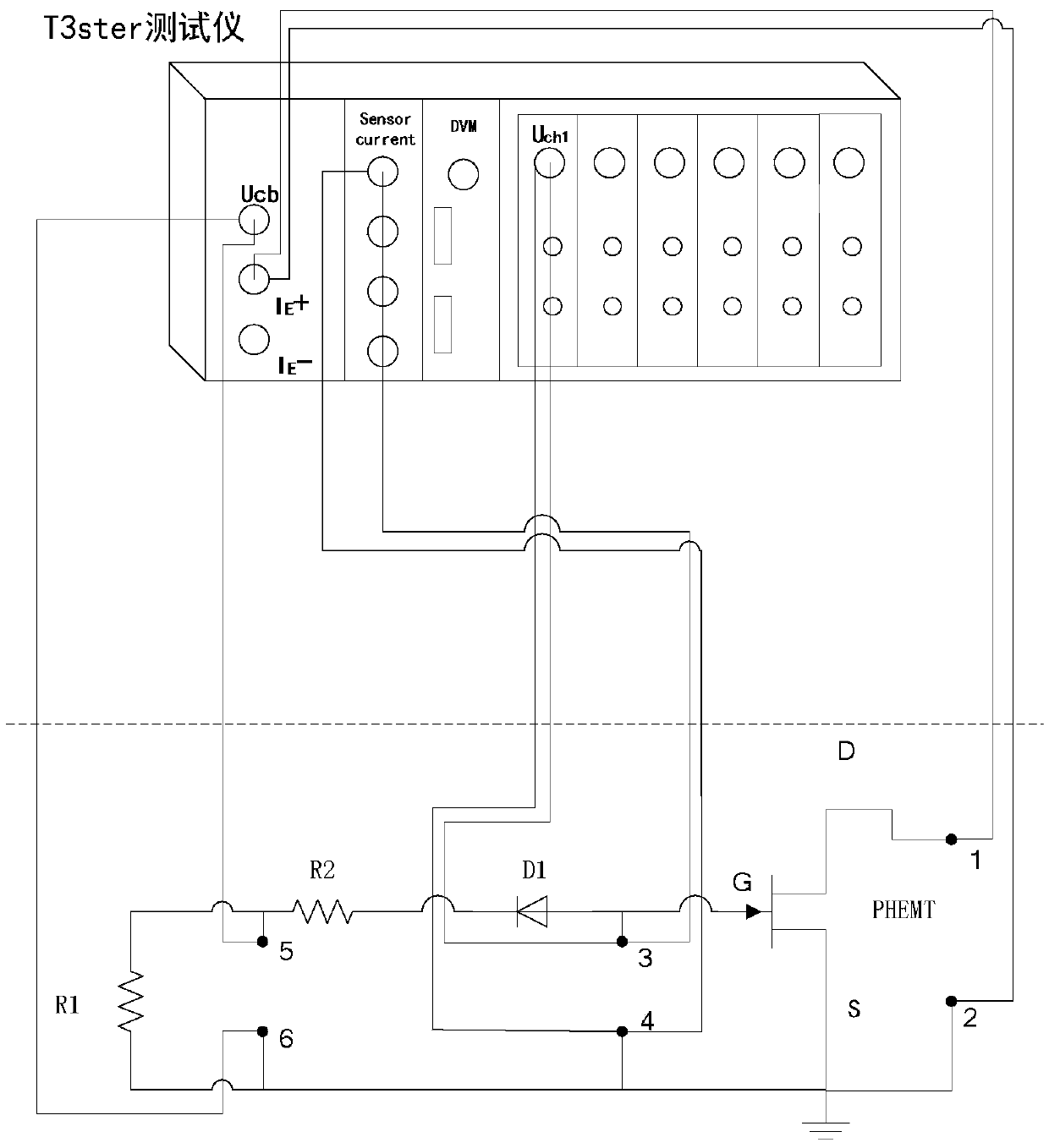
[0024] refer to figure 1 . In the embodiments described below, the peripheral control circuit is below the dotted line, and the commercial T3ster semiconductor thermal resistance tester is above the dotted line. High electron mobility transistor PHEMT thermal resistance testing device, including: PHEMT thermal resistance testing circuit and peripheral control circuit for thermal resistance testing of PHEMT using semiconductor thermal resistance testing instrument T3ster, wherein: PHEMT thermal resistance testing circuit consists of two voltage divider resistors R1, R2 and the fast recovery diode FRD are connected in series with the gate G of the PHEMT transistor. The anode IE+ of T3ster is electrically connected to the drain D of the PHEMT and the resistor R1 respectively through the terminal contacts 1 and 2 between the drain D and the source S of the PHEMT transistor. , the voltage output terminal Ucb is electrically connected to the terminal contact 5 between the resistor ...


PUM


Abstract

The invention discloses a heat resistance measurement method for a pseudomorphic high electron mobility transistor (PHEMT); by adopting the heat resistance measurement method, the temperature measurement is accurate, and damage to the PHEMT and measurement errors are not easy to cause. The method is implemented by the following technical scheme: a semiconductor heat resistance measurement instrument T3ster provides a current source to load current between a drain electrode and a source electrode of the PHEMT; a channel of the PHEMT is heated by the internal resistance of the transistor, then a T3ster peripheral control circuit performs instantaneous circuit switching, and the heating is stopped instantaneously; in the process, a voltage output end Ucb of the T3ster enables a fast recovery diode to be positively biased, under the effect of partial voltage of a divider resistor R1 connected with the Ucb on the Ucb, pinch-off voltage between a grid electrode G and the source electrode S of the PHEMT to be measured is generated, and reversal of biasing between the grid electrode G and the source electrode S of the PHEMT is realized; after the circuit switching, positive biasing between the grid electrode G and the source electrode S is realized, and the voltage drop reflects a temperature. Heat resistance is obtained according to a temperature change value measured by the T3ster by using data processing software Master of the T3ster in a computer.

Description

technical field [0001] The invention relates to the field of thermal testing of semiconductors, and relates to a measuring device for measuring the thermal resistance of a high electron mobility transistor PHEMT chip and a testing method thereof. Background technique [0002] The high electron mobility transistor PHEMT is the core device in the solid-state amplifier circuit. High electron mobility transistor PHEMT, as a kind of field effect transistor, has been widely used in communication and other fields due to its advantages of high frequency, high speed, low noise, and high power. As a sensitive unit, it is mostly used to make gas sensors and radio frequency power sensor. PHEMT is actually the title of a type of field effect tube chip, although there is a Schottky shield formed by the process that can be used for electrical temperature measurement, that is, Schottky. However, due to the characteristics of the Schottky, it cannot carry a large current, and cannot use th...

Claims


Application Information

Patent Timeline
IPC IPC(8): G01R31/26G01N25/20
CPCG01N25/20G01R31/2601
Inventor 胡家渝
Owner 10TH RES INST OF CETC
Learn More