Substrate, display panel and manufacturing method for substrate
A substrate and color film substrate technology, applied in nonlinear optics, instruments, optics, etc., can solve the problems of PCT test accuracy and product reliability, and achieve the effect of improving accuracy
- Summary
- Abstract
- Description
- Claims
- Application Information
AI Technical Summary
Problems solved by technology
Method used
Image
Examples
Embodiment 1
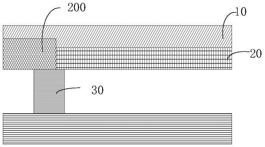
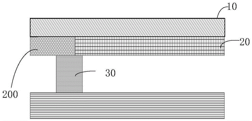
[0037] Figures 1A-1E A schematic structural view of the first embodiment of the substrate of the present invention is shown.
[0038] The substrate of the first embodiment of the present invention includes a substrate main body 10 and a planarization layer 20 disposed on the substrate main body 10, wherein the side of the substrate facing the liquid crystal layer has a notch 200, the notch 20 runs through the planarization layer 20, and the notch The gap 200 extends inward from the edge of the substrate, and at least part of the area is located in the sealant coating area, and the gap 200 is filled with a waterproof material.
[0039] Such as Figures 1A-1D As shown, the substrate of this embodiment has different forms of notch structures according to actual needs, and the following implementation manners are possible. For example, the boundary of the notch 200 in this embodiment extending along the plane where the planarization layer is located may only partially overlap wi...
Embodiment 2
[0044] figure 2 A schematic structural view of the second embodiment of the substrate of the present invention is shown.
[0045] Such as figure 2 As shown, the substrate of the first embodiment of the present invention includes a substrate body 10, and a planarization layer 20 disposed on the substrate body 10, wherein the side of the substrate facing the liquid crystal layer has a groove 201, and the groove 201 runs through the planarization layer. layer 20, and part of the groove 201 is located in the sealant coating area, and the groove 201 is filled with a waterproof material.
[0046] In this embodiment, the bottom of the groove 201 protrudes into the substrate main body 10, so that the waterproof material in the groove 201 divides the planarization layer 20 into two parts, and since a part of the groove 201 is located on the sealant coating area, so that after the cell is aligned, the planarization layer located inside the liquid crystal cell is isolated from the ou...
Embodiment 3
[0048] image 3 A schematic structural view of a third embodiment of the substrate of the present invention is shown.
[0049] Such as image 3 As shown, the difference between the substrate of this embodiment and the substrate of the first embodiment lies in the setting position and size of the groove. In this embodiment, the depth of the groove 201 is equal to the thickness of the planarization layer 20, that is, in the manufacturing process and etching part of the sealant-coated area of the planarization layer 20 to form grooves.
[0050] In this embodiment, the depth of the groove 201 is set equal to the thickness of the planarization layer 20 , so that the groove can be formed only by etching the planarization layer during manufacture, and the structure of the substrate body is not damaged.
PUM
 Abstract
Description
Claims
Application Information
 - R&D
- Intellectual Property
- Life Sciences
- Materials
- Tech Scout
- Unparalleled Data Quality
- Higher Quality Content
- 60% Fewer Hallucinations
Browse by: Latest US Patents, China's latest patents, Technical Efficacy Thesaurus, Application Domain, Technology Topic, Popular Technical Reports.
© 2025 PatSnap. All rights reserved.Legal|Privacy policy|Modern Slavery Act Transparency Statement|Sitemap|About US| Contact US: help@patsnap.com


