Preparation method of flexible surface enhanced Raman spectrum substrate and application thereof
A Raman spectrum substrate and flexible surface technology, applied in the direction of Raman scattering, material analysis through optical means, measurement devices, etc., can solve the problems of high cost, inability to detect in situ, and difficulty in preparing extremely small structures. consistent effect
- Summary
- Abstract
- Description
- Claims
- Application Information
AI Technical Summary
Problems solved by technology
Method used
Image
Examples
preparation example Construction
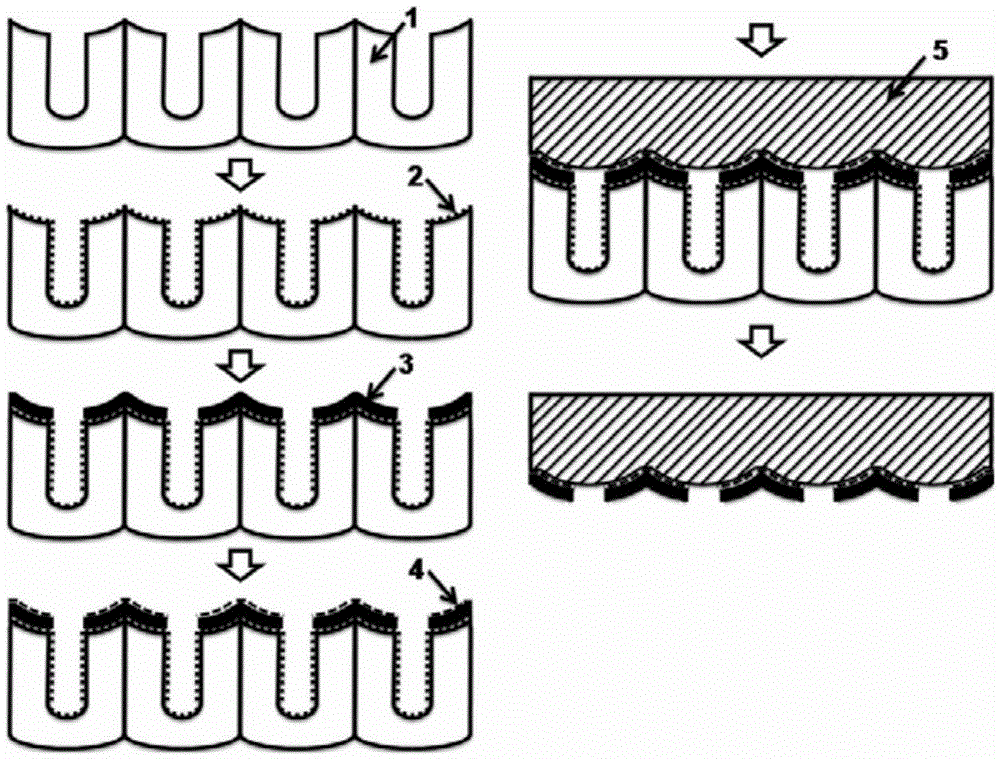
[0028] The general steps of the preparation method of the flexible surface-enhanced Raman spectroscopy substrate of the present invention are as follows: first, a layer of low surface energy material is coated on the surface of the anodized aluminum template, and then the active metal material layer and the metal adhesion layer are directly deposited, and then A flexible organic material support layer is prepared on the surface of the coating, and finally the organic material support layer with the active metal layer is separated from the surface of the anodized aluminum template to obtain a flexible surface-enhanced Raman spectrum substrate.
[0029] The schematic flow chart of the preparation method of the flexible surface-enhanced Raman spectrum substrate of the present invention is as attached figure 1 shown.
Embodiment 1
[0032] The steps of regulating the size of aluminum nanoparticles in this embodiment are as follows:
[0033] S1. A two-step anodic oxidation method is used to prepare a single-pass porous alumina template. The pore diameter, pore spacing and template thickness are 30nm, 100nm and 2000nm respectively; the surface of the anodized alumina template is coated with a layer of low surface energy material Alkylsilane.
[0034] S2. Deposit a layer of gold on the surface of the anodized aluminum template coated with low surface energy materials by electron beam evaporation, the deposition rate is 0.05nm / s, and the deposition thickness is 20nm.
[0035] S3. Evaporate a layer of chromium on the metal surface by electron beam evaporation, the deposition rate is 0.03nm / s, and the deposition thickness is 5nm.
[0036] S4. Prepare a layer of polydimethylsiloxane on the surface of the metal adhesion layer, and the thickness of the cured polydimethylsiloxane is 2 mm.
[0037]S5. After the or...
Embodiment 2
[0039] In this embodiment, the steps for preparing a flexible Raman-enhanced substrate are as follows:
[0040] S1. A two-step anodic oxidation method is used to prepare a single-pass porous alumina template. The pore diameter, pore spacing and template thickness are 30nm, 100nm and 2000nm respectively; the surface of the anodized alumina template is coated with a layer of low surface energy material Alkylsilanes.
[0041] S2. Deposit a layer of gold on the surface of the anodized aluminum template coated with low surface energy materials by electron beam evaporation, the deposition rate is 0.05nm / s, and the deposition thickness is 20nm.
[0042] S3. Prepare a polydimethylsiloxane film with a thickness of 1 mm.
[0043] S4. Coating a layer of self-assembled monolayer film based on mercapto group on the polydimethylsiloxane film to strengthen the adsorption force between the surface and gold. The anodized aluminum and the film are pressed together with a certain pressure for ...
PUM
| Property | Measurement | Unit |
|---|---|---|
| thickness | aaaaa | aaaaa |
| thickness | aaaaa | aaaaa |
| thickness | aaaaa | aaaaa |
Abstract
Description
Claims
Application Information
 - R&D
- Intellectual Property
- Life Sciences
- Materials
- Tech Scout
- Unparalleled Data Quality
- Higher Quality Content
- 60% Fewer Hallucinations
Browse by: Latest US Patents, China's latest patents, Technical Efficacy Thesaurus, Application Domain, Technology Topic, Popular Technical Reports.
© 2025 PatSnap. All rights reserved.Legal|Privacy policy|Modern Slavery Act Transparency Statement|Sitemap|About US| Contact US: help@patsnap.com


