Thin film transistor and array substrate

A technology of thin film transistor and ohmic contact layer, which is applied to transistors, electric solid state devices, semiconductor devices, etc., can solve the problems of increasing the difficulty of the array substrate process, reducing the production efficiency of the array substrate, etc., and achieving the effect of reducing leakage current.

Active Publication Date: 2016-03-16
TCL CHINA STAR OPTOELECTRONICS TECH CO LTD
View PDF4 Cites 3 Cited by
  • Summary
  • Abstract
  • Description
  • Claims
  • Application Information

AI Technical Summary

Problems solved by technology

However, this solution increases the difficulty of manufacturing the array substrate and reduces the production efficiency of the array substrate

Method used


Image

  • Thin film transistor and array substrate
  • Thin film transistor and array substrate
  • Thin film transistor and array substrate

Examples


Embodiment Construction

[0031] The implementation of the present invention will be described in detail below in conjunction with the accompanying drawings and examples, so as to fully understand and implement the process of how to apply technical means to solve technical problems and achieve technical effects in the present invention. It should be noted that, as long as there is no conflict, each embodiment and each feature in each embodiment of the present invention can be combined with each other, and the formed technical solutions are all within the protection scope of the present invention.

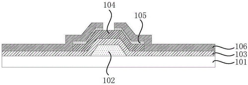
[0032] figure 1 A schematic structural diagram of an existing thin film transistor is shown.

[0033] Such as figure 1 As shown, the existing thin film transistor includes: a glass substrate 101 , a gate 102 , a gate insulating layer 103 , an active layer 104 , an ohmic contact layer 105 and a source / drain 106 . Wherein, the gate 102 is formed on the glass substrate 101 , and its constituent material is co...


PUM


Abstract

The invention discloses a thin film transistor and an array substrate. The thin film transistor comprises a grid electrode, a grid electrode insulation layer, an active layer, a first material layer and a source / drain electrode, wherein the grid electrode insulation layer is formed on the grid electrode and covers the grid electrode; the active layer is formed on the grid electrode insulation layer; the first material layer is formed on the active layer; the source / drain electrode is formed on the first material layer; the first material layer comprises a first Ohmic contact layer, a second Ohmic contact layer and a high-impedance inclusion layer, wherein the high-impedance inclusion layer is formed between the first Ohmic contact layer and the second Ohmic contact layer; and the impedance of the high-impedance inclusion layer is greater than the impedance of the first Ohmic contact layer and the second Ohmic contact layer. The thin film transistor can effectively lower leakage current which is in the presence between the source / drain electrode and the active layer and has a simple manufacture technology.

Description

technical field [0001] The present invention relates to the field of display technology, in particular to a thin film transistor and an array substrate. Background technique [0002] With the development of flat panel display (Flat Panel Display, FPD for short) technology, people have higher and higher requirements on display resolution and picture refresh rate, so the development of new materials and new processes is imminent. [0003] At present, in the field of Thin Film Transistor-Liquid Crystal Display (TFT-LCD for short), aluminum and molybdenum are the main metal materials of the conductive layer. The advantages of aluminum and molybdenum are that the film forming process is simple, the adhesion and flatness are good, the softness is not easy to cause climbing and disconnection, and it is not easy to spread to cause film pollution. Aluminum is the ideal conductive metal material of choice for small size and low resolution display panels. [0004] However, the resist...

Claims


Application Information

Patent Timeline
IPC IPC(8): H01L29/786H01L29/45H01L27/12
CPCH01L29/45H01L29/786H01L29/78669H01L27/1214H01L29/456
Inventor 孙涛
Owner TCL CHINA STAR OPTOELECTRONICS TECH CO LTD
Why Eureka
Try Eureka