Welding clamp for semiconductor photosensitive piece

A technology for welding fixtures and photosensitive parts, which is applied to semiconductor devices, welding equipment, auxiliary welding equipment, etc., can solve the problems of low processing efficiency and difficult positioning of semiconductor photosensitive parts, and achieve the effects of convenient operation, simple structure and easy realization.

Inactive Publication Date: 2016-03-09
重庆触视科技有限公司
View PDF7 Cites 0 Cited by
  • Summary
  • Abstract
  • Description
  • Claims
  • Application Information

AI Technical Summary

Problems solved by technology

[0004] The present invention intends to provide a welding fixture for semiconductor photosensitive parts to solve the problems of difficult positioning and low processing efficiency of existing semiconductor photosensitive parts during parallel welding

Method used


Image

  • Welding clamp for semiconductor photosensitive piece
  • Welding clamp for semiconductor photosensitive piece

Examples


Embodiment Construction

[0013] The present invention will be described in further detail below by means of specific embodiments:

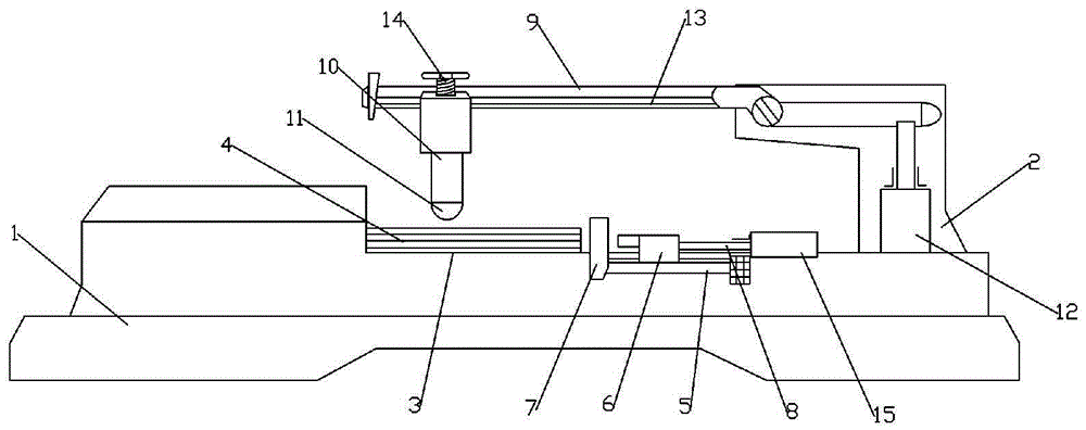
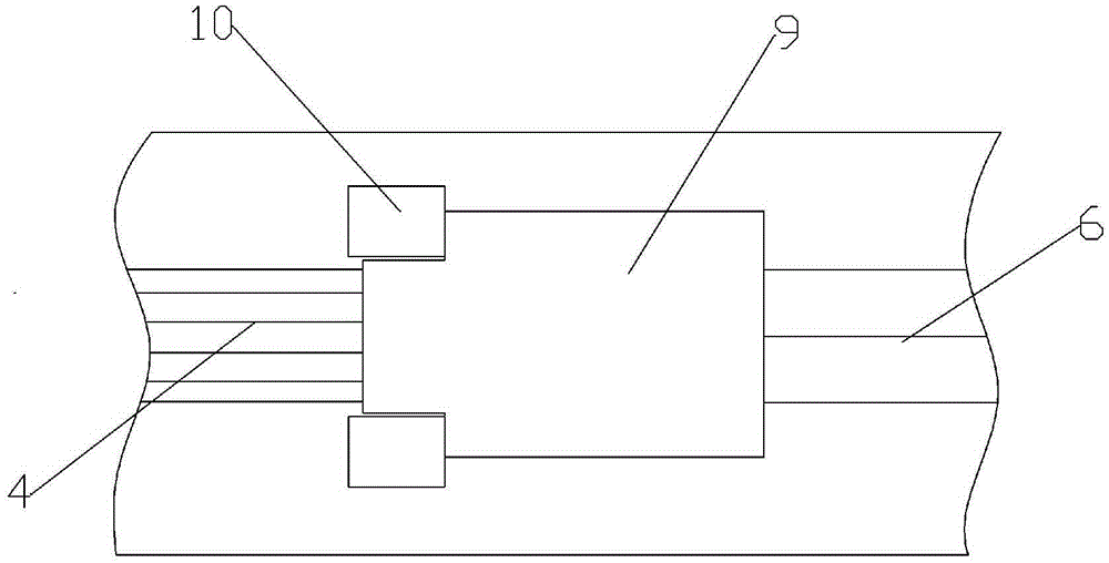
[0014] The reference signs in the drawings of the description include: base 1, frame 2, workbench 3, pin groove 4, horizontal slide rail 5, positioning block 6, limit block 7, pole 8, cantilever 9, strut 10 , Pressure head 11, second cylinder 12, chute 13, locking bolt 14, first cylinder 15.

[0015] The embodiment is basically as attached figure 1 , figure 2 Shown: the welding fixture of the semiconductor photosensitive element, including the base 1 and the frame 2 located on the base 1, the base 1 is provided with a workbench 3, and the workbench 3 is provided with tubes matching the pins of the semiconductor photosensitive element The pin groove 4 and the pin groove 4 are a number of needle grooves arranged horizontally. The workbench 3 is provided with a horizontal slide rail 5, and a positioning block 6 slidingly connected to the horizontal slide rail 5 is provide...


PUM


Abstract

The invention provides a welding clamp for a semiconductor photosensitive piece, which comprises a base and a rack arranged on the base, wherein a working table is arranged on the base; a pin slot matched with a pin of the semiconductor photosensitive piece is formed in the working table; a horizontal sliding rail is arranged on the working table; an inverted T-shaped positioning block, which is connected with the horizontal sliding rail in a sliding way, is arranged on one side of the pin slot; a limiting block for limiting the positioning block is arranged between the horizontal sliding rail and the pin slot; the positioning block is connected with a plunger rod; the plunger rod is connected with a first air cylinder mounted on the base; a cantilever is hinged to the rack; a support rod located above the pin slot is arranged at one end of the cantilever; the support rod is connected with a pressing head for pressing the semiconductor photosensitive piece; and a second air cylinder mounted on the rack is arranged at the other end of the cantilever. The welding clamp aims to solve the problem that the conventional semiconductor photosensitive piece is hard to position and low in processing efficiency during parallel welding.

Description

technical field [0001] The invention relates to the technical field of photoelectric device processing equipment, in particular to a welding fixture for semiconductor photosensitive parts. Background technique [0002] Photoconductive devices that utilize the photosensitive properties of semiconductors, photovoltaic cells and semiconductor light-emitting devices that utilize semiconductor photovoltaic effects are collectively referred to as optoelectronic devices. Optoelectronic devices mainly include: photoconductive devices that use the photosensitive properties of semiconductors, photocells and semiconductor photosensitive devices that use semiconductor photovoltaic effects to work. Semiconductor optoelectronic devices such as light pipes, photocells, photodiodes, phototransistors, etc.; semiconductor thermoelectric devices such as thermistors, thermoelectric generators, and thermoelectric coolers. [0003] Semiconductor photosensitive devices are photoconductive devices...

Claims


Application Information

Patent Timeline
IPC IPC(8): B23K37/04
CPCB23K37/0443B23K2101/40
Inventor 任博
Owner 重庆触视科技有限公司
Why Eureka
Try Eureka