The Circuit Structure and Method of Realizing Clock Recovery Based on USB Device
A clock recovery and circuit structure technology, applied in electrical components, pulse processing, pulse technology, etc., can solve the problems of complex peripheral, large circuit area, poor jitter suppression performance, etc., to simplify peripheral circuits, wide application range, reduce product cost effect
- Summary
- Abstract
- Description
- Claims
- Application Information
AI Technical Summary
Problems solved by technology
Method used
Image
Examples
Embodiment Construction
[0056] In order to describe the technical content of the present invention more clearly, further description will be given below in conjunction with specific embodiments.
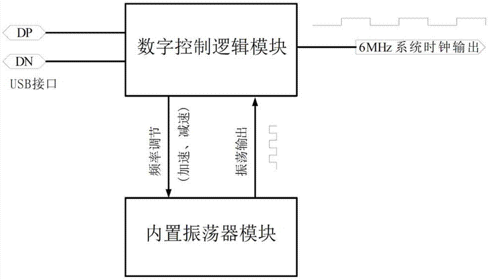
[0057] The present invention is mainly composed of a built-in oscillator module and a digital control logic module, such as figure 1 shown.
[0058] The built-in oscillator module is used to generate an oscillation signal much higher than 1.5MHz as the clock signal of the digital control logic module;
[0059] The digital control logic module is firstly used to sample the clock signal generated by the built-in oscillator module for the duration of the 4th and 5th bits (sampling bits) of the USB interface synchronous signal to complete clock recovery; secondly, the digital control logic module also compares the USB data Transmission frequency and the frequency of the built-in oscillator, automatically switch the frequency of the built-in oscillator between low speed, medium speed and high speed.
[0060] T...
PUM
 Abstract
Description
Claims
Application Information
 - R&D
- Intellectual Property
- Life Sciences
- Materials
- Tech Scout
- Unparalleled Data Quality
- Higher Quality Content
- 60% Fewer Hallucinations
Browse by: Latest US Patents, China's latest patents, Technical Efficacy Thesaurus, Application Domain, Technology Topic, Popular Technical Reports.
© 2025 PatSnap. All rights reserved.Legal|Privacy policy|Modern Slavery Act Transparency Statement|Sitemap|About US| Contact US: help@patsnap.com


