Semiconductor device and manufacturing method thereof, and electronic device

A manufacturing method and semiconductor technology, applied in semiconductor devices, semiconductor/solid-state device manufacturing, electric solid-state devices, etc., can solve problems such as uneven thickness of tunneling oxide layers, achieve good breakdown voltage, and improve device coupling rate Effect

Active Publication Date: 2016-02-17
SEMICON MFG INT (SHANGHAI) CORP
View PDF3 Cites 3 Cited by
  • Summary
  • Abstract
  • Description
  • Claims
  • Application Information

AI Technical Summary

Problems solved by technology

This will result in a severely non-uniform thickness of the tunnel oxide layer, with the thickness of the tunnel oxide layer at the edge of the active region being thinner than that in the middle of the active region

Method used


Image

  • Semiconductor device and manufacturing method thereof, and electronic device
  • Semiconductor device and manufacturing method thereof, and electronic device
  • Semiconductor device and manufacturing method thereof, and electronic device

Examples


Embodiment 1

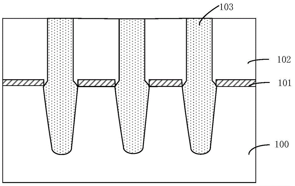
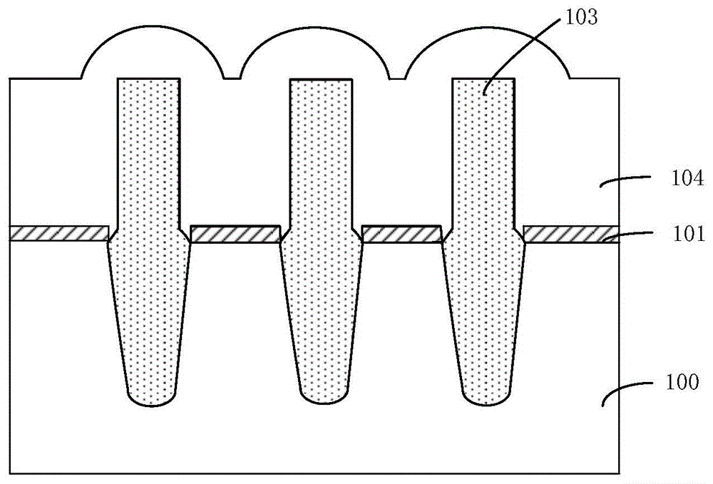
[0039] The following will combine Figures 2A-2G Describe in detail the manufacturing method of the embedded flash memory of the present invention, Figures 2A-2G It is a cross-sectional view of the structure of the memory in the process of fabricating the embedded flash memory according to an embodiment of the present invention.

[0040] Such as Figure 2A As shown, a semiconductor substrate 200 is provided in which a well is formed.

[0041]The semiconductor substrate may be at least one of the materials mentioned below: silicon, silicon-on-insulator (SOI), silicon-on-insulator (SSOI), silicon-germanium-on-insulator (S-SiGeOI), silicon-on-insulator Silicon germanium (SiGeOI) and germanium on insulator (GeOI), etc. As an example, in this embodiment, single crystal silicon is selected as the constituent material of the semiconductor substrate.

[0042] The semiconductor substrate 200 includes three regions, namely: a first region for forming a logic circuit gate structure,...

Embodiment 2

[0084] According to the manufacturing method of the present invention, a semiconductor device is also provided, and the semiconductor device includes a floating gate with a T-shaped structure.

[0085] Exemplarily, the bottom width of the floating gate is 50 nm to 75 nm, and the top width of the floating gate is 60 nm to 110 nm.

Embodiment 3

[0087] An embodiment of the present invention provides an electronic device, which includes a semiconductor device. Wherein, the semiconductor device is the semiconductor device described in Embodiment 2, or the semiconductor device manufactured according to the method for manufacturing a semiconductor device described in Embodiment 1.

[0088] The electronic device of this embodiment can be any electronic product or equipment such as mobile phone, tablet computer, notebook computer, netbook, game console, TV set, VCD, DVD, navigator, camera, video recorder, voice recorder, MP3, MP4, PSP, etc. , can also be any intermediate product including semiconductor devices. The electronic device according to the embodiment of the present invention has better performance due to the use of the above-mentioned semiconductor device.


PUM

PropertyMeasurementUnit
Bottom widthaaaaaaaaaa
Top widthaaaaaaaaaa
Thicknessaaaaaaaaaa

Abstract

The invention discloses a semiconductor device and a manufacturing method thereof, and an electronic device. The method comprises the following steps: forming a hard mask layer on a semiconductor substrate; etching the hard mask layer and the semiconductor substrate so as to form a shallow trench; filling an isolation material layer in the shallow trench; removing the hard mask layer; forming a tunneling oxide layer on the exposed semiconductor substrate; forming a first floating gate material layer on the semiconductor substrate; executing a planarization technology; forming a second floating gate material layer whose width is greater than that of the first floating gate material layer on the first floating gate material layer by use of an epitaxial growth technology; and successively forming a dielectric layer and a control gate material layer on the semiconductor substrate. According to the manufacturing method provided by the invention, a good technical window is provided for forming a shallow trench isolation structure oxide layer and floating gate polysilicon.

Description

technical field [0001] The invention relates to a semiconductor manufacturing process, in particular to an embedded flash memory and a manufacturing method thereof. Background technique [0002] Memory is used to store a large amount of digital information. According to recent surveys, memory chips account for about 30% of semiconductor transactions worldwide. Over the years, technological progress and market demand have resulted in more and more high-density various type memory. [0003] Random access memory, such as DRAM and SRAM (static random access memory), has the problem of data loss after power failure during use. To overcome this problem, various nonvolatile memories have been designed and developed. Recently, flash memory based on floating gate concept has become the most general non-volatile memory due to its small cell size and good performance. [0004] Flash memory is FLASH, which has become the mainstream of non-volatile semiconductor storage technology. Am...

Claims


Application Information

Patent Timeline
IPC IPC(8): H01L21/28H01L21/762H01L21/8247H01L29/423H01L27/115H01L27/11521
Inventor 王新鹏
Owner SEMICON MFG INT (SHANGHAI) CORP
Why Eureka
Try Eureka