A wafer bonding method

A wafer and bonding technology, which is applied in the photoengraving process of the pattern surface, the process for producing decorative surface effects, and decorative arts, etc. The effect of avoiding cracking, improving yield and improving effectiveness

Active Publication Date: 2017-08-04
WUHAN XINXIN SEMICON MFG CO LTD
View PDF6 Cites 0 Cited by
  • Summary
  • Abstract
  • Description
  • Claims
  • Application Information

AI Technical Summary

Problems solved by technology

Due to the warping of the wafer bonded edge, in the subsequent processing process, when the upper wafer is thinned, cracks and other defects are prone to appear on the wafer bond or sidewall, which greatly reduces the yield of the product

Method used


Image

  • A wafer bonding method
  • A wafer bonding method
  • A wafer bonding method

Examples


specific Embodiment approach

[0043] A specific embodiment is listed: this embodiment is only an embodiment of the present invention, and is not intended to specifically limit the present invention.

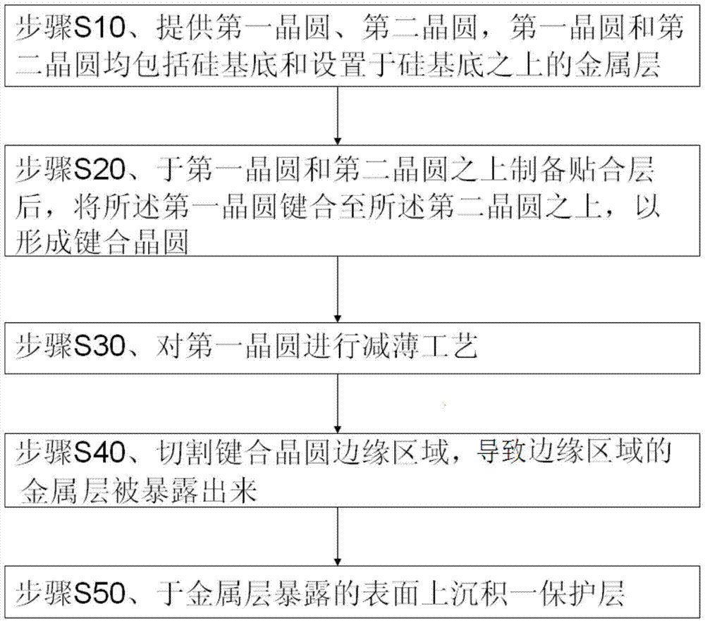
[0044] Such as Figure 2a As shown, two wafers to be bonded are provided. Here, for the convenience of description, the two wafers are respectively referred to as a first wafer and a second wafer.

[0045] Such as Figure 2b As shown, first, the bonding layers of the two wafers are bonded to each other. That is, the bonding layer of the first wafer is bonded and connected to the bonding layer of the second wafer.

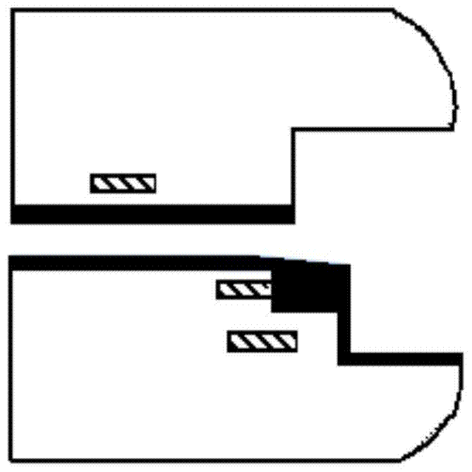
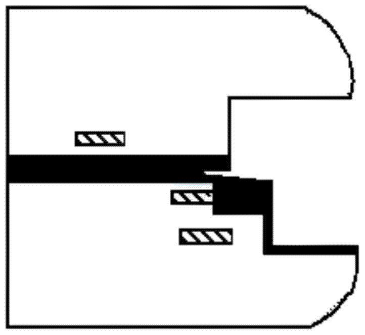
[0046] Such as Figure 2c As shown, thinning treatment is performed on the surface of the first wafer at the upper end to remove the silicon deposition layer with a predetermined thickness. At the same time, during the thinning process, a retracted incision chamfer is produced on the bonding layer. The retracted type The shape of the notch chamfer is different due to the different processes use...


PUM


Abstract

The present invention relates to the technical field of semiconductor manufacturing, and in particular to a method for bonding wafers. The specific steps are: providing a first wafer and a second wafer, and both the first wafer and the second wafer include a silicon substrate and a wafer. a metal layer disposed on the silicon substrate; after preparing a bonding layer on the first wafer and the second wafer, bonding the first wafer to the second wafer to form a bonded wafer; performing a thinning process on the first wafer; cutting the edge area of ​​the bonded wafer to expose the metal layer in the edge area; depositing a protective layer on the exposed surface of the metal layer. By cutting the bonding layer of the edge area of ​​the two wafers to form a flat side wall, it is also conducive to the release of the stress inside the wafer, so as to avoid the damage caused by the stress release inside the wafer during the packaging process. Round edges are warped. Make the surface of the bonded wafer in a completely flat state, improve the effectiveness of bonding, eliminate the cracks on the edge and side wall of the bonded wafer, and improve the yield of products.

Description

technical field [0001] The invention relates to the technical field of semiconductor manufacturing, in particular to a wafer bonding method. Background technique [0002] Wafer bonding technology refers to the method of tightly combining two wafers through chemical and physical effects. Wafer bonding is often combined with surface silicon processing and bulk silicon processing, and is used in the processing technology of MEMS. Although wafer bonding is not a direct means of micromachining, it plays an important role in micromachining. By combining with other processing methods, it can not only provide support and protection for microstructures, but also realize the mechanical structure between mechanical structures or mechanical structures. An electrical connection to a circuit. The quality of wafer bonding will have a direct impact on the performance of the micromechanical system, and the warpage of the wafer before and after bonding is one of the main factors affecting th...

Claims


Application Information

Patent Timeline
Patent Type & Authority Patents(China)
IPC IPC(8): B81C3/00B81C1/00
Inventor 穆钰平周玉曹静胡胜孙鹏
Owner WUHAN XINXIN SEMICON MFG CO LTD
Why Eureka
Try Eureka