Adjustable and controllable preparation method for large-area nanometer microstructure of fused quartz optical curved face

A technology of fused silica and microstructure, which is applied in the field of nano-manufacturing, can solve the problems of accurate control and inability to realize the cycle of microstructure, and achieve the effect of improving performance, low requirements for motion resolution and positioning accuracy, and stable structure

Active Publication Date: 2016-01-27
NAT UNIV OF DEFENSE TECH
View PDF4 Cites 2 Cited by
  • Summary
  • Abstract
  • Description
  • Claims
  • Application Information

AI Technical Summary

Problems solved by technology

However, there are still related technical problems in the application of ion beam processing technology to the preparation of microstructures: on the one hand, the relationship between ion beam processing parameters and microstructures is not yet clear, and it is impossible to accurately control the characteristics of microstructures such as period and amplitude On the other hand, the application of ion beam processing to the preparation of microstructures on curved surfaces (especially high-steep curved surfaces) has important significance for the applicability of processing technology

Method used


Image

  • Adjustable and controllable preparation method for large-area nanometer microstructure of fused quartz optical curved face
  • Adjustable and controllable preparation method for large-area nanometer microstructure of fused quartz optical curved face
  • Adjustable and controllable preparation method for large-area nanometer microstructure of fused quartz optical curved face

Examples


Embodiment Construction

[0038] The following will be based on the caliber The fused silica optical curved surface optical part with a vertex curvature radius of 16 mm is used as the fused silica optical curved surface optical part to be processed, and the method for preparing the large-area nano-microstructure control of the fused silica optical curved surface of the present invention is further specifically described.

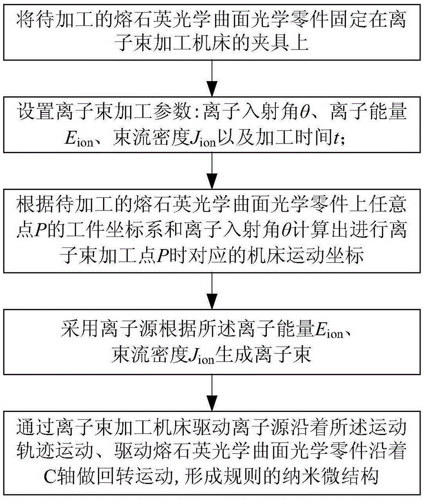
[0039] Such as figure 1 As shown, the steps of the large-area nano-microstructure control preparation method of the fused silica optical curved surface in this embodiment include:

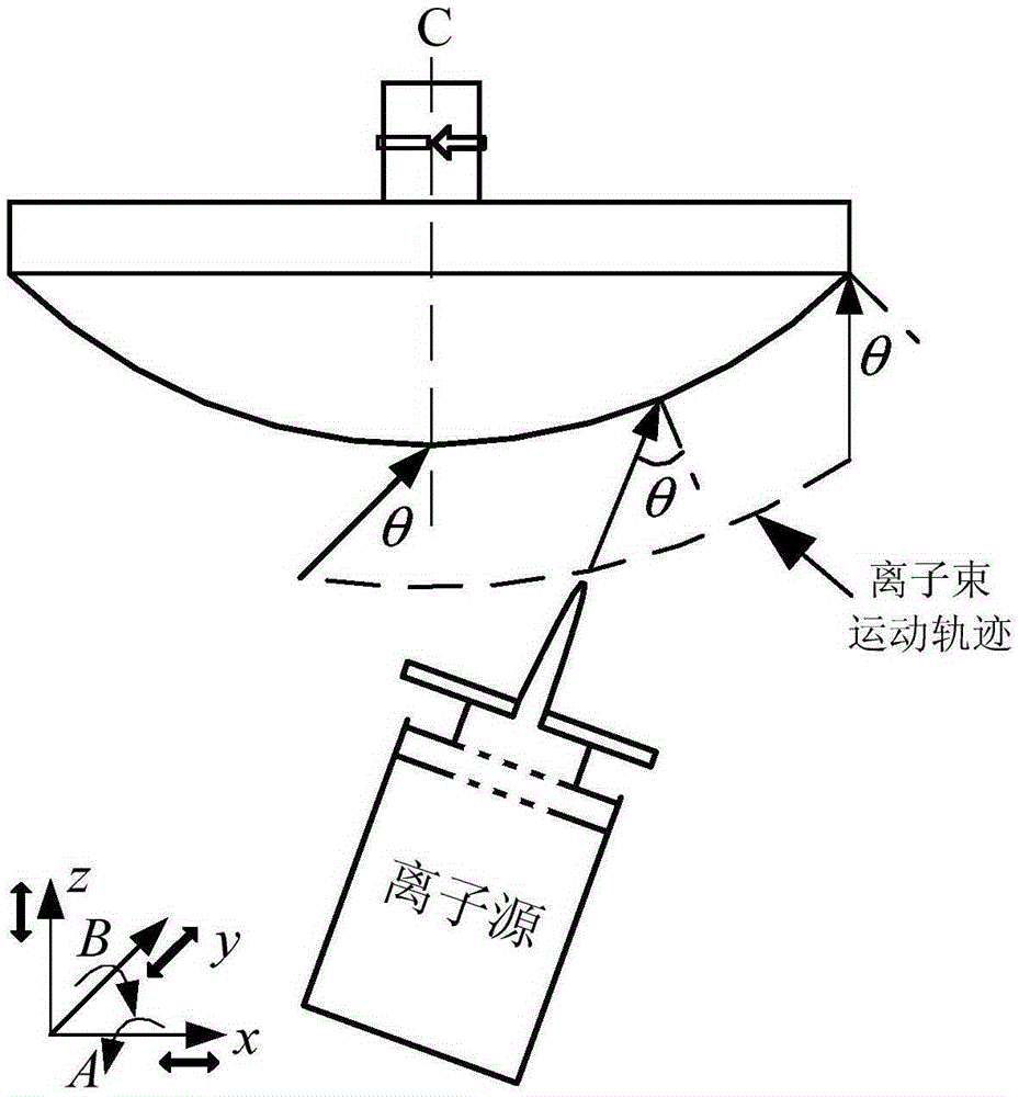
[0040] 1) Fix the fused silica optical curved surface optical part to be processed on the fixture of the ion beam processing machine tool, and the fixture is connected to the ion beam processing machine tool through a motor that can drive the fused silica optical curved surface optical part to perform rotary motion along the C axis ,Such as figure 2 shown;

[0041] 2) set the ion beam processing para...


PUM


Abstract

The invention discloses an adjustable and controllable preparation method for a large-area nanometer microstructure of a fused quartz optical curved face. The method comprises the following steps: fixing a fused quartz optical curved face optical part; setting an ion incident angle theta, an ion energy E<ion>, a beam current density J<ion> and a machining time t; determining a motion track of ion beam machining performed on the fused quartz optical curved face optical part; and generating ion beams through an ion source according to the ion energy E<ion> and the beam current density J<ion>, driving the ion source to move along the motion track through an ion beam machining tool, and driving the fused quartz optical curved face optical part to perform revolving motions along a C axis in order that the ion beams enter the curved face of the fused quartz optical curved face optical part at the fixed ion incident angle theta for an incidence time t, thereby forming a regular nanometer microstructure on the curved face of the fused quartz optical curved face optical part finally. The method is particularly suitable for adjustable and controllable preparation of the large-area nanometer microstructure of the fused quartz curved face, and has the advantages of simple principle, easiness in implementation, high efficiency and low cost.

Description

technical field [0001] The invention relates to the technical field of nano-manufacturing, in particular to a large-area nano-microstructure control preparation method of a fused silica optical curved surface. Background technique [0002] The preparation and control technology of ordered microstructures has gradually attracted widespread attention, and has important research significance and application value in modern science and technology. Its application range includes many high-tech fields such as optical devices, integrated circuits, and micro-electromechanical systems. In order to meet the increasing demand of related technologies for the preparation of microstructures, scholars at home and abroad have conducted in-depth research on related preparation methods, resulting in rapid development of the preparation technology of microstructures. [0003] However, with the development and progress of science and technology, the preparation of microstructures is developing ...

Claims


Application Information

Patent Timeline
Patent Type & Authority Applications(China)
IPC IPC(8): B81C1/00
Inventor 戴一帆廖文林解旭辉周林徐明进鹿迎
Owner NAT UNIV OF DEFENSE TECH
Why Eureka
Try Eureka