Planar heterojunction sensitized organic fluorescence light-emitting diode and preparation method therefor
A light-emitting diode and heterojunction technology, applied in semiconductor/solid-state device manufacturing, electrical components, electric solid-state devices, etc., can solve problems such as short service life of blue phosphorescent OLED devices, difficulty in reducing device driving voltage, and cumbersome device preparation process, etc. , to achieve the effect of reducing material cost, reducing material types, and less preparation process
- Summary
- Abstract
- Description
- Claims
- Application Information
AI Technical Summary
Problems solved by technology
Method used
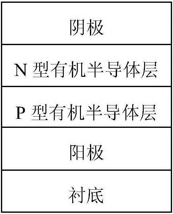
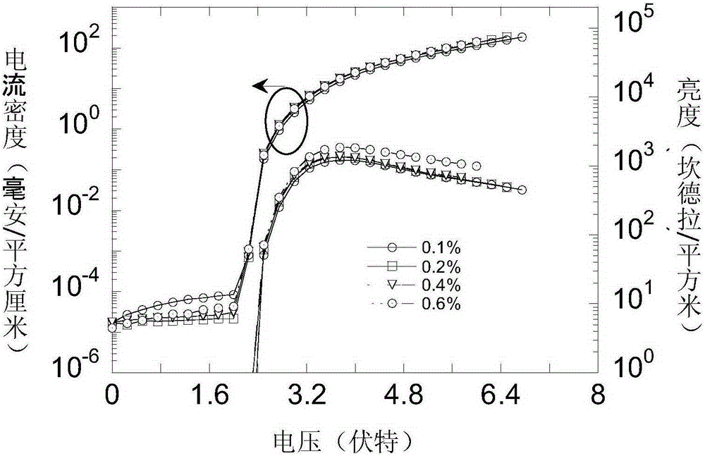
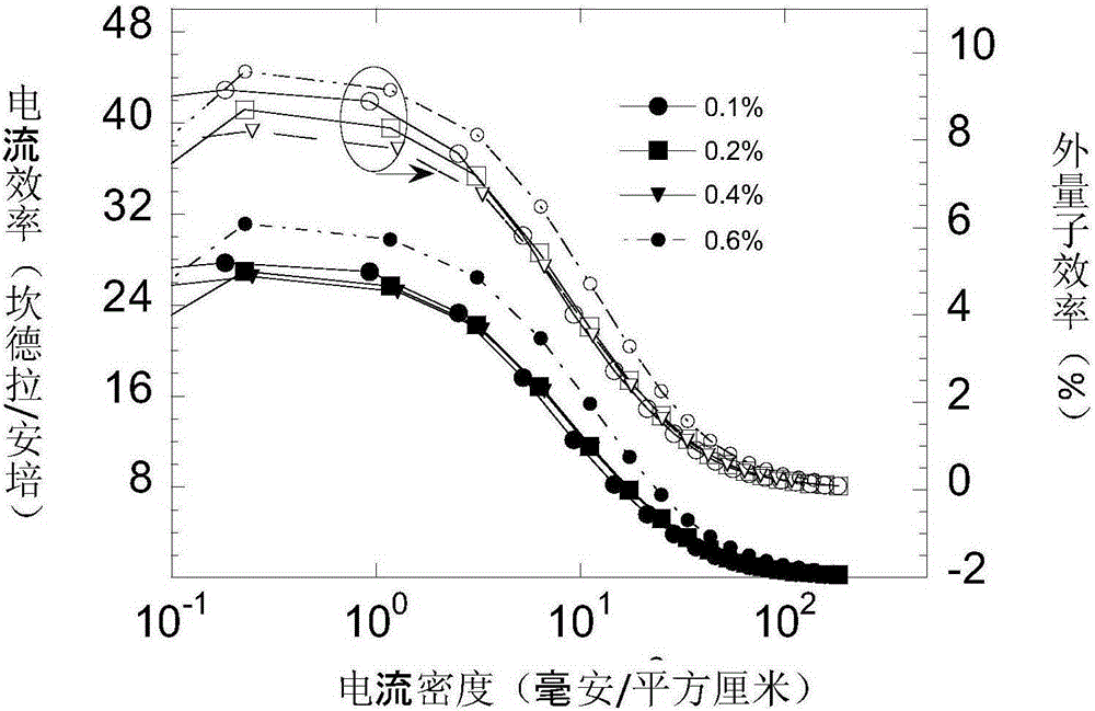
Image

Examples
Embodiment 1
[0046]Take a number of ITO conductive glass substrates with the same batch number, the size is 30 mm × 30 mm, the thickness of ITO is about 90 nanometers, and its square resistance is about 20 ohms / square. Sequentially use acetone, special detergent for micron semiconductors, deionized water, and isopropanol to ultrasonically clean for 15 minutes to remove dirt on the surface of the substrate. Then put it into an incubator and dry it at 80 degrees Celsius for later use. The dried ITO substrate was treated with plasma ignition equipment for 4 minutes to further remove organic pollutants attached to the surface. Then the ITO substrate was transferred to an anhydrous and oxygen-free glove box filled with high-purity nitrogen. In this glove box, the devices are loaded into the vacuum plating chamber. Turn on the mechanical pump and molecular pump, when the plating chamber reaches 4×10 -4 After the high vacuum, the thermal evaporation film starts. Using a specific mask, sequent...
Embodiment 2
[0051] The preparation process is the same as in Example 1 but without the anode buffer layer, and the P-type organic semiconductor materials are respectively selected as DMQA-doped TAPC (the doping concentration is 0.7%, molar ratio) and DMQA-doped TCTA (the doping concentration is 1.1%, molar ratio), the N-type organic semiconductor material is TmPyTZ doped with DMQA (doping concentration is 0.7%, molar ratio). Control the thickness of the P-type organic semiconductor material layer to be 25 nanometers and the thickness of the N-type organic semiconductor material layer to be 60 nanometers to obtain planar heterojunction sensitized organic fluorescent light-emitting diodes: ITO glass substrate / DMQA doped TAPC (25 nano) / DMQA-doped TmPyTZ (60 nm) / LiF (1 nm) / Al (device 1) and ITO glass substrate / DMQA-doped TCTA (25 nm) / DMQA-doped TmPyTZ (60 nm) / fluorine Lithium oxide (1 nm) / aluminum (device 2). The device is a device type in which a double-sided P-type semiconductor material a...
PUM
 Abstract
Description
Claims
Application Information
 - Generate Ideas
- Intellectual Property
- Life Sciences
- Materials
- Tech Scout
- Unparalleled Data Quality
- Higher Quality Content
- 60% Fewer Hallucinations
Browse by: Latest US Patents, China's latest patents, Technical Efficacy Thesaurus, Application Domain, Technology Topic, Popular Technical Reports.
© 2025 PatSnap. All rights reserved.Legal|Privacy policy|Modern Slavery Act Transparency Statement|Sitemap|About US| Contact US: help@patsnap.com