
LED pixel arrangement structure, printing type display device and preparation method of display device

A technology of light-emitting diodes and pixel arrangement, which is used in identification devices, static indicators, instruments, etc., can solve the problems of decreased resolution of display devices, low resolution of pixel structures, and is not suitable for printing and preparation. The effect of improving the resolution and improving the service life

Inactive Publication Date: 2016-01-20
深圳市TCL高新技术开发有限公司
View PDF5 Cites 43 Cited by
  • Summary
  • Abstract
  • Description
  • Claims
  • Application Information

AI Technical Summary

Problems solved by technology

[0004] The purpose of the present invention is to provide a light-emitting diode pixel arrangement structure, which aims to solve the problem of low resolution and poor stability of the pixel structure caused by the increase in the number of sub-pixels, and is not suitable for printing preparation.
[0005] Another object of the present invention is to provide a printed display device including the above-mentioned light-emitting diode pixel arrangement structure, aiming to solve the problem that the resolution of the display device decreases due to the increase in the number of sub-pixels in the printing process

Method used


Image

  • LED pixel arrangement structure, printing type display device and preparation method of display device
  • LED pixel arrangement structure, printing type display device and preparation method of display device
  • LED pixel arrangement structure, printing type display device and preparation method of display device

Examples


Embodiment Construction

[0025] In order to make the technical problems, technical solutions and beneficial effects to be solved by the present invention clearer, the present invention will be further described in detail below in conjunction with the accompanying drawings and embodiments. It should be understood that the specific embodiments described here are only used to explain the present invention, not to limit the present invention.

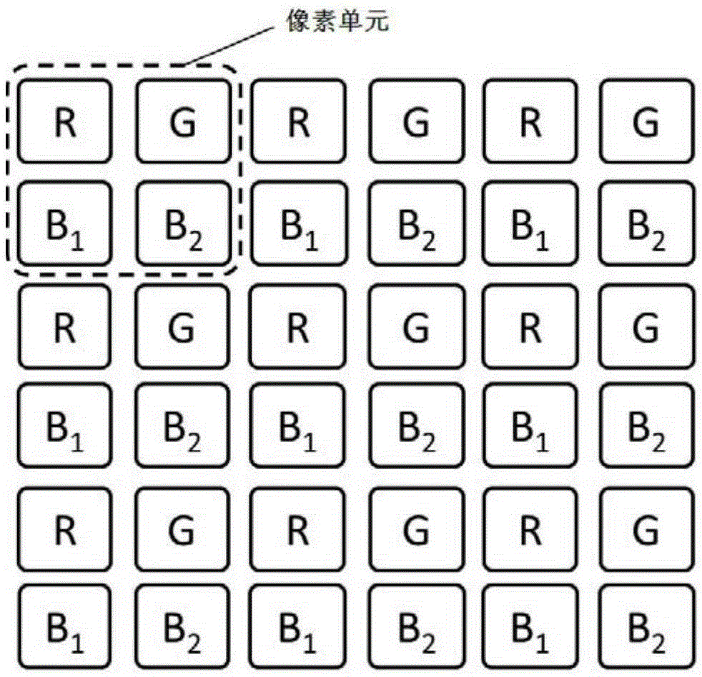
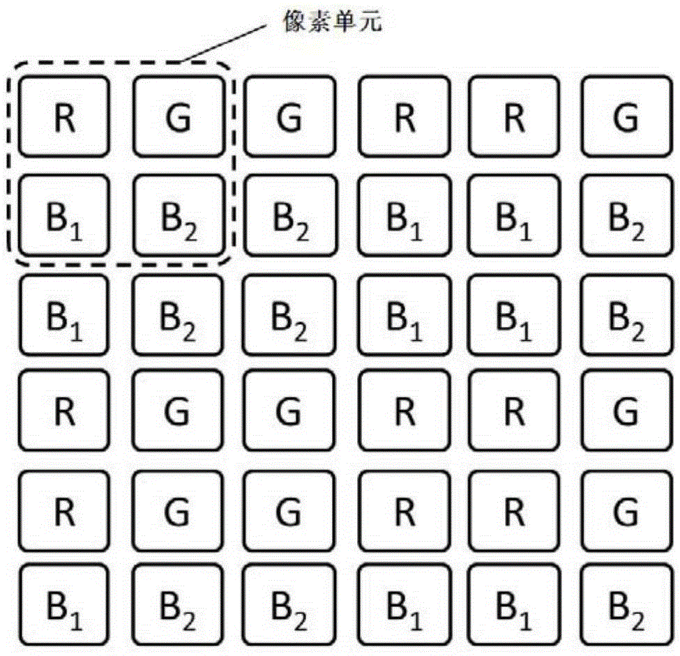
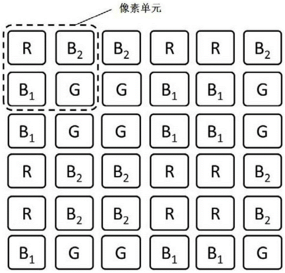
[0026] combine Figure 2-4 , an embodiment of the present invention provides a light-emitting diode pixel arrangement structure, including a plurality of pixel units, the pixel unit includes four sub-pixels of different colors: R, G, B1, B2, the R, G, B1, B2 respectively represent red sub-pixels, green sub-pixels, sky blue sub-pixels and dark blue sub-pixels, the sub-pixels of four different colors in the pixel unit are arranged in a 2×2 rectangular shape, and the pixel unit is 2×2 Any group of vertical sides of the rectangle constructs an x-y coordinate axis, and...


PUM

PropertyMeasurementUnit
Thicknessaaaaaaaaaa
Thicknessaaaaaaaaaa

Abstract

The invention provides an LED pixel arrangement structure, a printing type display device with the LED pixel arrangement structure and a preparation method of the display device, and suitable for the field of display technology. The LED pixel arrangement structure comprises multiple pixel units, each pixel unit comprises four different colors of sub pixels, namely a red sub pixel R, a green sub pixel G, a sky blue sub pixel B1 and a dark blue sub pixel B2, the sub pixels of four different colors in the same pixel unit are in 2*2 rectangular arrangement, a random vertical side of the 2*2 rectangle is used to construct a reference axis of the x-y system, the pixel unit are in mirror symmetry in the axis x and axis y directions, and the sub pixels of the same color of connected pixel units form a same-color sub pixel area in 2*2 arrangement.

Description

technical field [0001] The invention belongs to the field of display technology, and in particular relates to a light-emitting diode pixel arrangement structure, a printing display device containing the light-emitting diode pixel arrangement structure and a preparation method thereof. Background technique [0002] Light-emitting diodes (LEDs) have received more and more attention due to their low energy consumption, low heat production, and long life in the contemporary era of strong awareness of environmental protection and energy conservation. They are gradually replacing traditional lighting technologies and becoming a new generation of lighting power supplies. . Among them, the organic electroluminescent diode (OLED) has the advantages of self-illumination, fast response, wide viewing angle, high brightness, and thinness, etc., and the quantum dot light-emitting diode (QLED) has the advantages of high light color purity, high luminous quantum efficiency, and easy-to-adju...

Claims


Application Information

Patent Timeline
IPC IPC(8): H01L27/32H01L27/12G09F9/33G09G3/32
CPCG09G3/32G09G2300/0426G09G2300/0452H10K59/353
Inventor 陈亚文
Owner 深圳市TCL高新技术开发有限公司
Learn More