Processing method of step groove circuit board and step groove circuit board
A processing method and stepped groove technology are applied in printed circuit, multi-layer circuit manufacturing, printed circuit manufacturing, etc. to achieve the effect of solving the connection between layers of stepped groove circuit boards
- Summary
- Abstract
- Description
- Claims
- Application Information
AI Technical Summary
Problems solved by technology
Method used
Image

Examples
Embodiment 1
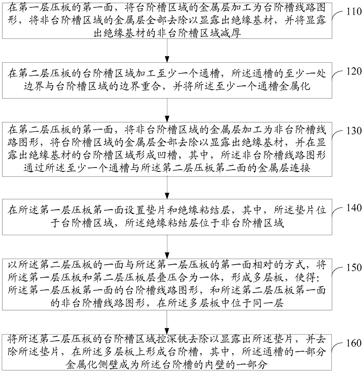
[0031] Please refer to figure 1 , an embodiment of the present invention provides a processing method for a stepped groove circuit board, which may include:
[0032] 110. On the first side of the first laminate, the metal layer in the stepped groove area is processed into a stepped groove circuit pattern, and all the metal layers in the non-step groove area are removed to reveal the insulating substrate, and the insulating substrate will be exposed. The non-step groove area is thickened.
[0033] In the embodiment of the present invention, for the step-slot circuit board to be processed, the step-slot circuit board is divided into two parts with the bottom plane of the step-slot as the interface, and the step-slot circuit board is manufactured separately. Each of these parts is pre-pressed into laminates, referred to as the first laminate and the second laminate, respectively. Wherein, each laminate includes: metal layers on two sides, at least one circuit layer in the middl...
Embodiment 2
[0055] Please refer to image 3 , Another method for processing a stepped groove circuit board according to an embodiment of the present invention may include:
[0056] 310. On the first side of the first laminate, the metal layer in the stepped groove area is processed into a stepped groove circuit pattern, and all the metal layers in the non-step groove area are removed to reveal the insulating substrate, and the insulating substrate will be exposed. The non-step groove area is thickened.
[0057] 320. Process through holes in the non-step groove regions of the second laminate, and metalize the through holes.
[0058] 330. On the first side of the second laminate, process the metal layer in the non-step groove area into a non-step groove circuit pattern, remove all the metal layers in the step groove area to reveal the insulating base material, and expose the insulating base A groove is formed in the stepped groove area of the material, wherein the non-step groove circui...
Embodiment 3
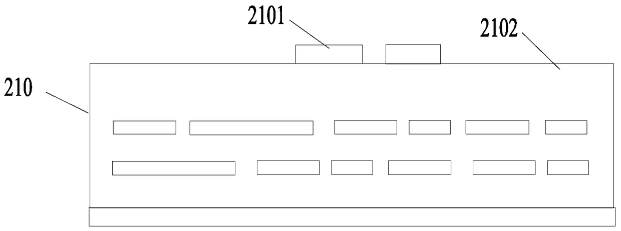
[0065] Please refer to Figure 2m , an embodiment of the present invention provides a stepped groove circuit board, one side of the stepped groove circuit board has a stepped groove 250, the bottom of the stepped groove 250 has a stepped groove circuit pattern 2101, and the inner wall of the stepped groove 250 has a metal Chemical plating layer, the non-step groove circuit pattern 2204 located on the same layer as the step groove circuit pattern 2101 passes through the metallized coating on the inner wall of the step groove 250, and the outer layer circuit with the step groove side of the step groove circuit board Graphical connection.
[0066] As can be seen from the above, the present invention discloses a step-slot circuit board, the step-slot circuit board is connected between layers through the metallized inner wall of the step-slot, so no metallized blind holes need to be processed, which solves the problem that blind holes cannot be used in the prior art. The technical...
PUM
 Abstract
Description
Claims
Application Information
 - Generate Ideas
- Intellectual Property
- Life Sciences
- Materials
- Tech Scout
- Unparalleled Data Quality
- Higher Quality Content
- 60% Fewer Hallucinations
Browse by: Latest US Patents, China's latest patents, Technical Efficacy Thesaurus, Application Domain, Technology Topic, Popular Technical Reports.
© 2025 PatSnap. All rights reserved.Legal|Privacy policy|Modern Slavery Act Transparency Statement|Sitemap|About US| Contact US: help@patsnap.com