An optical module, its signal output port, and a signal output port protection circuit
A signal output and protection circuit technology, which is applied in the direction of logic circuits using optoelectronic devices, logic circuits using specific components, reliability improvement and modification, etc., can solve problems such as damage to optical module chips, and achieve the effect of preventing damage from breakdown
- Summary
- Abstract
- Description
- Claims
- Application Information
AI Technical Summary
Problems solved by technology
Method used
Image

Examples
Embodiment 1
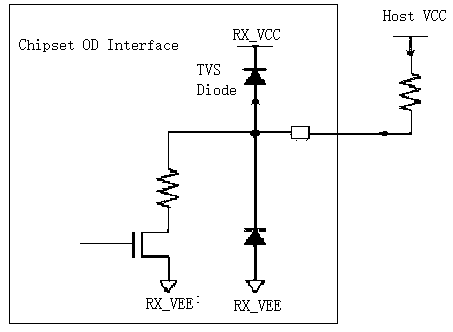
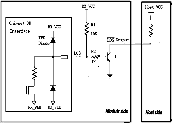
[0038] Embodiment 1: as figure 2 As shown, this embodiment provides an optical module signal output port OC protection circuit, including:
[0039] The input terminal is connected to the base of the first transistor T1 through the second resistor R2, and is used to receive the output signal LOS of the signal output port of the optical module chip;
[0040] a pull-up power supply RX_VCC, connected to the input terminal through a first resistor R1, and used to provide a pull-up voltage for the base of the first transistor T1;
[0041] The first transistor T1, the emitter of the first transistor T1 is grounded; the collector of the first transistor T1 is the output terminal of the OC protection circuit, and the output terminal is connected to the input port on the host side.
[0042] When the output signal LOS of the signal output port of the optical module chip is high level or low level, when its output is low level, the first transistor T1 is turned off. At this time, due to...
Embodiment 2
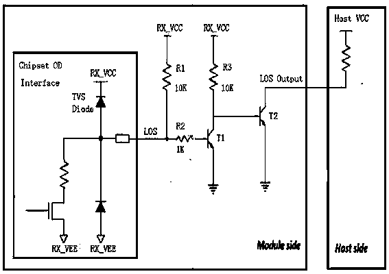
[0044] Embodiment 2: as image 3 As shown, on the basis of Embodiment 1, the OC protection circuit provided in this embodiment also includes,
[0045] The second transistor T2, the emitter of the second transistor T2 is grounded; the base of the second transistor T2 is connected to the collector of the first transistor T1; the collector of the second transistor T2 is protected by the OC The output end of the circuit, the output end is connected to the input port on the host side;
[0046] The third resistor R3 is arranged between the pull-up power supply and the base of the second transistor T2, and is used for providing a pull-up voltage to the base of the second transistor T2.
[0047] The effect of adding the second transistor T2 is to make the output of the protection circuit consistent with the output of the signal output port of the optical module chip; that is, when the output signal LOS of the signal output port of the optical module chip is low, the first The transi...
Embodiment 3
[0049] Embodiment 3: as figure 2 As shown, the present invention provides an optical module signal output port at the same time, the optical module signal output port includes an optical module chip signal output port, and an OC protection circuit is externally connected to the optical module chip signal output port; The OC includes a circuit that includes an input terminal connected to the base of the first transistor T1 through a second resistor R2 for receiving the output signal LOS of the signal output port of the optical module chip; a pull-up power supply connected to the input terminal through the first resistor R1 Terminal connection, used to provide a pull-up voltage for the base of the first transistor T1; the first transistor T1, the emitter of the first transistor T1 is grounded; the collector of the first transistor T1 is the OC protection circuit The output terminal is connected to the input port on the host side.
PUM
 Abstract
Description
Claims
Application Information
 - R&D
- Intellectual Property
- Life Sciences
- Materials
- Tech Scout
- Unparalleled Data Quality
- Higher Quality Content
- 60% Fewer Hallucinations
Browse by: Latest US Patents, China's latest patents, Technical Efficacy Thesaurus, Application Domain, Technology Topic, Popular Technical Reports.
© 2025 PatSnap. All rights reserved.Legal|Privacy policy|Modern Slavery Act Transparency Statement|Sitemap|About US| Contact US: help@patsnap.com