
Inner layer bonding pad later-windowed rigid-flexible printed circuit board and manufacturing method thereof

A technology of soft and hard combination board and inner layer, which is applied in the direction of multi-layer circuit manufacturing, printed circuit manufacturing, electrical components, etc., can solve the problems of reduced yield rate, low yield rate, increased production cost, etc., and achieve high efficiency and high yield rate High and yield-enhancing effects

Active Publication Date: 2015-12-09
SHENZHEN HUALIN CIRCUIT TECH
View PDF5 Cites 28 Cited by
  • Summary
  • Abstract
  • Description
  • Claims
  • Application Information

AI Technical Summary

Problems solved by technology

Disadvantages: There are many production processes of soft and hard boards, the production is difficult, the yield rate is low, the input materials and manpower are more, and the production cycle is relatively long
However, with this process, the process is increased by about 20%, and two more layers of adhesive layers and two layers of pure copper foil are required than the previous method, which reduces the yield rate and increases production costs, reducing market competitiveness.

Method used


Image

  • Inner layer bonding pad later-windowed rigid-flexible printed circuit board and manufacturing method thereof
  • Inner layer bonding pad later-windowed rigid-flexible printed circuit board and manufacturing method thereof
  • Inner layer bonding pad later-windowed rigid-flexible printed circuit board and manufacturing method thereof

Examples


Embodiment Construction

[0031] The invention provides a method for manufacturing a rigid-flex board with a rear opening of an inner pad, comprising the following steps:

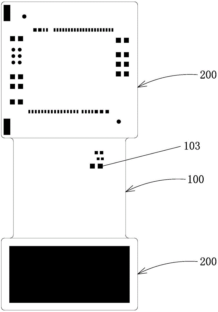
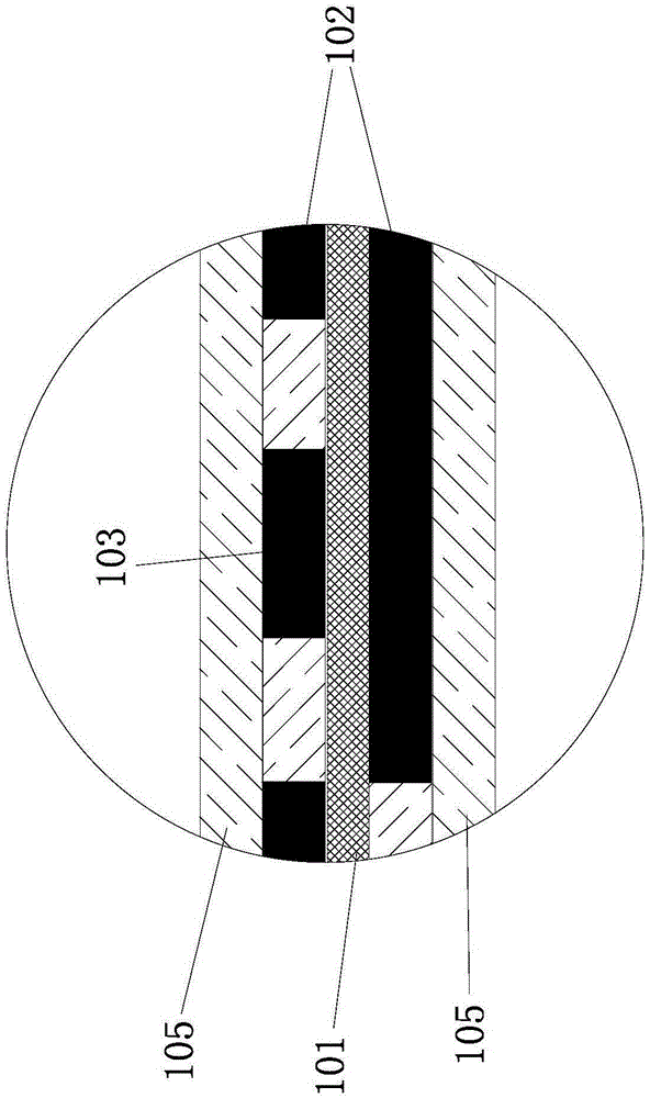
[0032] S1. FPC base material 101 is cut, drilled, and copper-plated. According to the circuit design requirements, the FPC copper layer 102 of the FPC base material 101 is etched to form an inner layer circuit, and at the same time, the window area 104 is etched according to the window opening requirements. For the corresponding inner layer pad 103, when etching to form the inner layer pad 103, it should be ensured that the window area 104 can fall within the range of the corresponding inner layer pad 103, and the inner layer cover film 105 without a window should be attached to the corresponding inner layer pad 103. The surface of the flexible board substrate 101 described above. In this step, the windowed area 104 of the inner covering film 105 is not pierced temporarily and passes through CO in a later step. 2 laser burn through...


PUM


Abstract

An inner layer bonding pad later-windowed rigid-flexible printed circuit board and a manufacturing method thereof. The manufacturing method includes the steps of: S1. cutting a flexible printed circuit board (FPC) base material, etching an FPC copper layer of the FPC base material to form an inner layer circuit according to a circuit design requirement, etching to form an inner layer bonding pad corresponding a windowing region according to a windowing requirement, the windowing region being guaranteed to fall in the range of the corresponding inner layer bonding pad when the inner layer bonding pad is formed by etching, and then gluing an inner layer covering film without a window on the surface of the FPC base material, thereby obtaining the FPC; S2. attaching an outer layer pure copper coil layer on a rigid printed circuit board base material and pressing the rigid printed circuit board base material in a rigid printed circuit board region of the FPC, thereby obtaining a rigid-flexible printed circuit board; and S3. using CO2 laser to perform windowing firing on a region that needs windowing of the inner layer covering film, and the windowing region being punched through and the inner layer bonding pad of the FPC being exposed, thereby obtaining the inner layer bonding pad later-windowed rigid-flexible printed circuit board. The manufacturing method provided by the invention has relatively high efficiency and yield.

Description

technical field [0001] The invention relates to a rigid-flex board for circuit boards used in digital products such as mobile phones and computers, in particular to a rigid-flex board with a window on the back of an inner pad and a manufacturing method thereof. Background technique [0002] The birth and development of FPC (flexible circuit board) and PCB (rigid board) gave birth to the new product of soft and hard board. Therefore, Rigid-Flexible Printed Circuit Board (R-FPCB) is a flexible circuit board and a rigid circuit board. After pressing and other processes, they are combined according to relevant process requirements to form a circuit board with FPC characteristics and PCB characteristics. . Advantages: The rigid-flex board has both the characteristics of FPC and PCB. Therefore, it can be used in some products with special requirements. It has both a certain flexible area and a certain rigid area, which is helpful for saving the internal space of the product. , I...

Claims


Application Information

Patent Timeline
IPC IPC(8): H05K1/11H05K3/46H05K3/40
CPCH05K1/0298H05K1/11H05K3/40H05K3/4691H05K2203/107
Inventor 潘陈华汪传林曹焕威
Owner SHENZHEN HUALIN CIRCUIT TECH
Learn More