Array substrate mother board and manufacturing method thereof, display panel and mother board

An array substrate and display panel technology, applied in static indicators, instruments, etc., can solve problems such as defective display panels and failure of display panels to perform normal detection, achieve high practical value, improve detection efficiency, and avoid mutual interference.

Active Publication Date: 2015-11-25
BOE TECH GRP CO LTD +1
View PDF5 Cites 6 Cited by
  • Summary
  • Abstract
  • Description
  • Claims
  • Application Information

AI Technical Summary

Problems solved by technology

[0004] Aiming at the defects in the prior art, the present invention provides an array substrate mother board and its manufacturing method, a display panel and the mother board, which can solve the defects that occur in the display panel during the detection process of the array substrate and cause defects on the display mother board. The problem that all display panels have the same abnormal phenomenon at the same time and cannot be detected normally

Method used


Image

  • Array substrate mother board and manufacturing method thereof, display panel and mother board
  • Array substrate mother board and manufacturing method thereof, display panel and mother board
  • Array substrate mother board and manufacturing method thereof, display panel and mother board

Examples


Embodiment Construction

[0023] In order to make the purpose, technical solutions and advantages of the embodiments of the present invention clearer, the technical solutions in the embodiments of the present invention will be clearly and completely described below in conjunction with the drawings in the embodiments of the present invention. Obviously, the described embodiments It is a part of embodiments of the present invention, but not all embodiments. Based on the embodiments of the present invention, all other embodiments obtained by persons of ordinary skill in the art without creative efforts fall within the protection scope of the present invention.

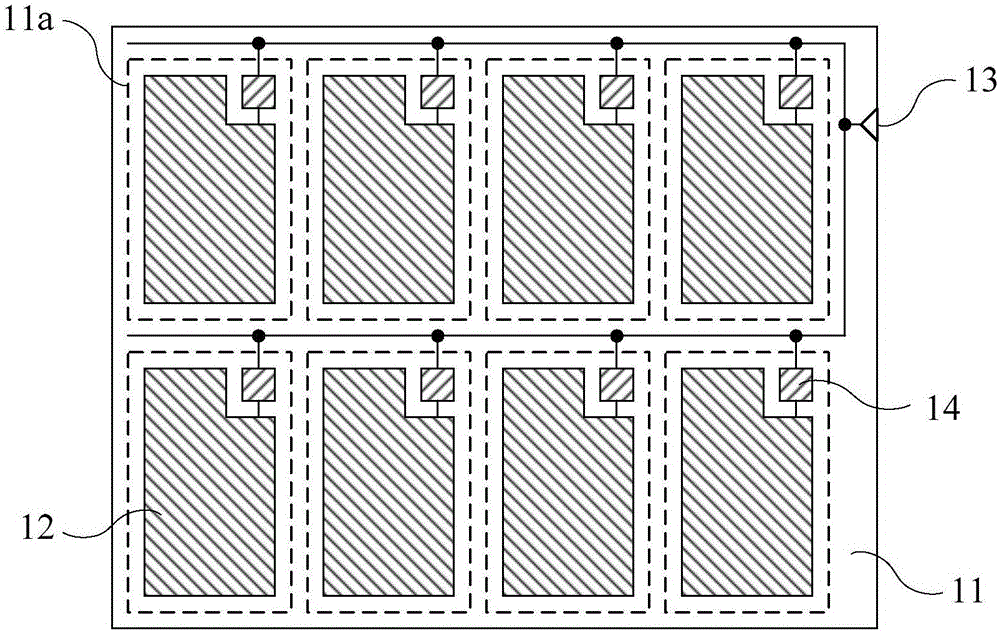
[0024] figure 1 It is a schematic diagram of the surface structure of an array substrate motherboard in an embodiment of the present invention. see figure 1 , the array substrate motherboard includes several display panel areas 11a, and a transistor circuit 12 is arranged in each display area 11a. It should be understood that the array substrat...


PUM


Abstract

The invention provides an array substrate mother board and a manufacturing method thereof, a display panel and a mother board. The array substrate mother board comprises a plurality of display panel areas, and a transistor circuit is arranged in each display area; corresponding to any external detection signal, the array substrate mother board is provided with an input terminal, and the input terminal is connected with a connection terminal for receiving the external detection signal in the transistor circuit of each display panel area through at least one one-way conducting circuit; and the one-way conducting circuit is used for transmitting the external detection signal. The invention can solve the problem that normal detection cannot be implemented because all display panels on the display mother board simultaneously produce the same abnormal phenomenon due to failure in a display panel in the detection process of an array substrate.

Description

technical field [0001] The present invention relates to the field of display technology, in particular to an array substrate motherboard and a manufacturing method thereof, a display panel and the motherboard. Background technique [0002] In the prior art, small-sized display panels (for example, below 18.5 inches) are usually mass-produced on the same large-sized substrate, and then individual products are formed from the produced display motherboard through cutting and other processes. During the manufacturing process, the circuit inspection of the array substrate in the display panel is usually performed in batches. Specifically, for a display motherboard including several display panels, an external detection signal can be transmitted to the detection of each display panel through a general input port of a detection signal set on the display motherboard and a corresponding transmission line. At the input end of the signal, the detection of all display panels can be com...

Claims


Application Information

Patent Timeline
Patent Type & Authority Applications(China)
IPC IPC(8): G09G3/00
Inventor 蔡振飞吴成业刘海峰
Owner BOE TECH GRP CO LTD
Why Eureka
Try Eureka