
Method for reducing the damage to a substrate surface in ONO etching

A substrate surface, substrate technology, applied in the direction of electrical components, semiconductor/solid-state device manufacturing, circuits, etc., can solve problems such as damage to the substrate surface 11

Inactive Publication Date: 2015-10-28
SHANGHAI HUAHONG GRACE SEMICON MFG CORP
View PDF6 Cites 2 Cited by
  • Summary
  • Abstract
  • Description
  • Claims
  • Application Information

AI Technical Summary

Problems solved by technology

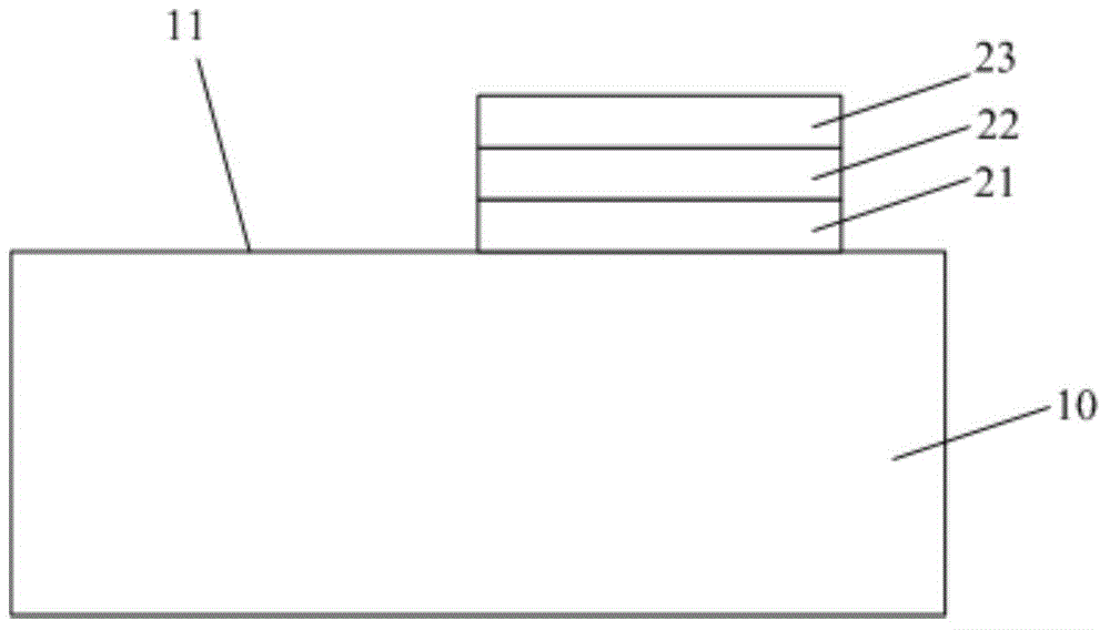
[0004] However, the existing problem is that if the first oxide layer 21 at the bottom of the ONO structure is too thin, the exposed part of the substrate surface 11 is likely to be damaged due to excessive dry etching

Method used


Image

  • Method for reducing the damage to a substrate surface in ONO etching
  • Method for reducing the damage to a substrate surface in ONO etching
  • Method for reducing the damage to a substrate surface in ONO etching

Examples


Embodiment Construction

[0022] In order to make the content of the present invention clearer and easier to understand, the content of the present invention will be described in detail below in conjunction with specific embodiments and accompanying drawings.

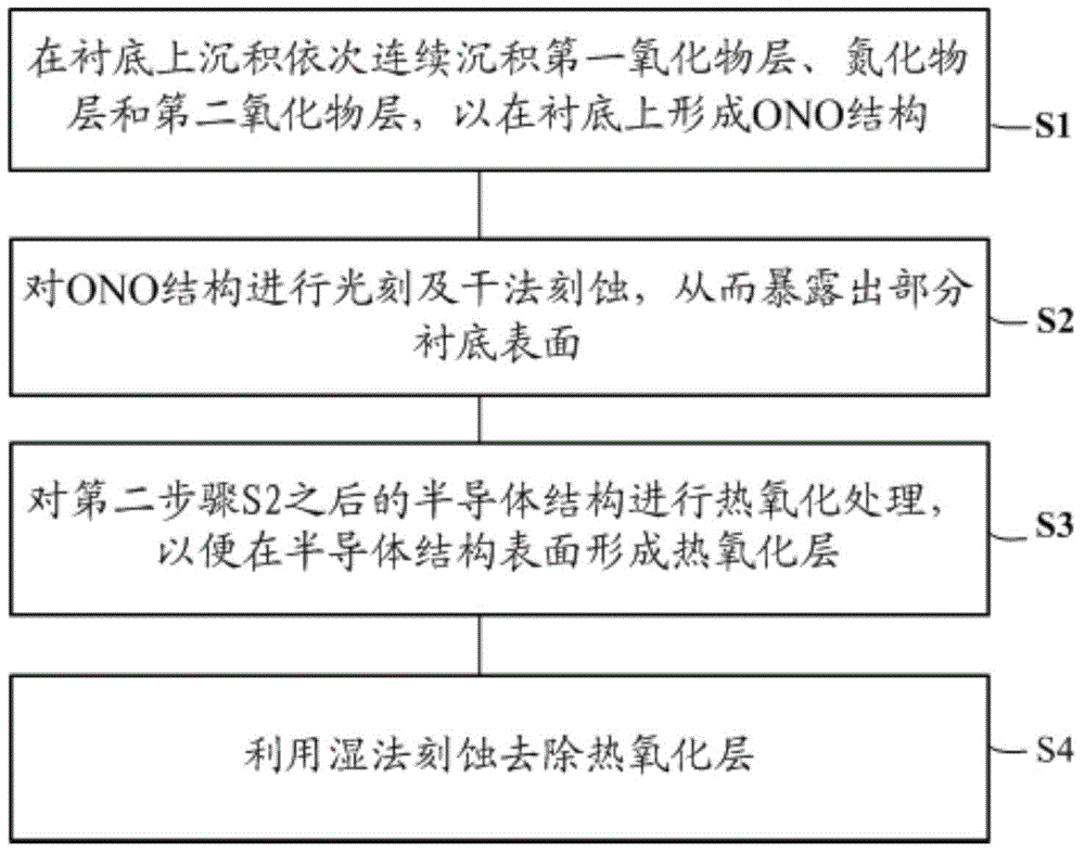
[0023] image 3 A flow chart of a method for reducing substrate surface damage in ONO etching according to a preferred embodiment of the present invention is schematically shown. and, Figure 4 to Figure 7 Each step of the method for reducing substrate surface damage in ONO etching according to a preferred embodiment of the present invention is schematically shown.

[0024] combine now Figure 4 to Figure 7 and refer to image 3 A method for reducing substrate surface damage in ONO etching according to a preferred embodiment of the present invention will be described.

[0025] The method for reducing substrate surface damage in ONO etching according to a preferred embodiment of the present invention includes:

[0026] The first step S1: fir...


PUM


Abstract

The invention provides a method reducing the damage to a substrate surface in ONO etching. The method comprises following steps; the first step, of depositing on a substrate successively a first oxide layer, a nitride layer and a second oxide layer to form an ONO structure on the substrate; the second step, of processing the ONO structure by the method of lithography and dry etching to expose the substrate surface; the third step, perform thermal oxidation treatment on the semiconductor structure after the second step to form a thermal oxidation layer on the surface of the semiconductor structure; the fourth step, of removing the thermal oxidation layer by a wet etching process.

Description

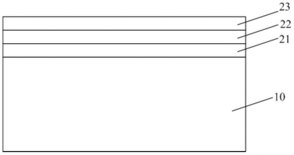
technical field [0001] The invention relates to the field of semiconductor manufacturing, more specifically, the invention relates to a method for reducing substrate surface damage in ONO etching. Background technique [0002] The ONO (Oxide-Nitride-Oxide, Oxide / Nitride / Oxide) structure is a structure that is often encountered in the manufacturing process of semiconductor devices. Moreover, ONO structures often need to be deposited and etched during semiconductor device fabrication. [0003] figure 1 and figure 2 The ONO etching steps according to the prior art are schematically shown. Such as figure 1 and figure 2 As shown, firstly, a first oxide layer 21 , a nitride layer 22 and a second oxide layer 23 are successively deposited on a substrate 10 (generally a silicon substrate) to form an ONO structure on the substrate 10 . The ONO structure is subsequently etched, thereby exposing part of the substrate surface 11 . [0004] However, the existing problem is that i...

Claims


Application Information

Patent Timeline
IPC IPC(8): H01L21/316
CPCH01L21/02164H01L21/02238H01L21/02255
Inventor 吴亚贞刘宪周
Owner SHANGHAI HUAHONG GRACE SEMICON MFG CORP
Learn More