Copper mixed bonding method

A hybrid bonding and pre-bonding technology, applied in the field of bonding, can solve problems such as the difficulty in realizing the internal interconnection of wafer metal circuits, and achieve the effects of reducing wire resistance and delay, and good process foundation

Active Publication Date: 2015-10-14
WUHAN XINXIN SEMICON MFG CO LTD
View PDF10 Cites 6 Cited by
  • Summary
  • Abstract
  • Description
  • Claims
  • Application Information

AI Technical Summary

Problems solved by technology

[0003] The technical problem to be solved by the present invention is to provide a copper hybrid bonding technology to solve the technical problem that it is difficult to realize the internal interconnection of metal circuits between wafers in the prior art

Method used


Image

  • Copper mixed bonding method
  • Copper mixed bonding method
  • Copper mixed bonding method

Examples


Embodiment Construction

[0027] The principles and features of the present invention are described below in conjunction with the accompanying drawings, and the examples given are only used to explain the present invention, and are not intended to limit the scope of the present invention.

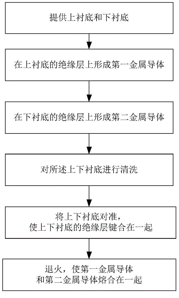
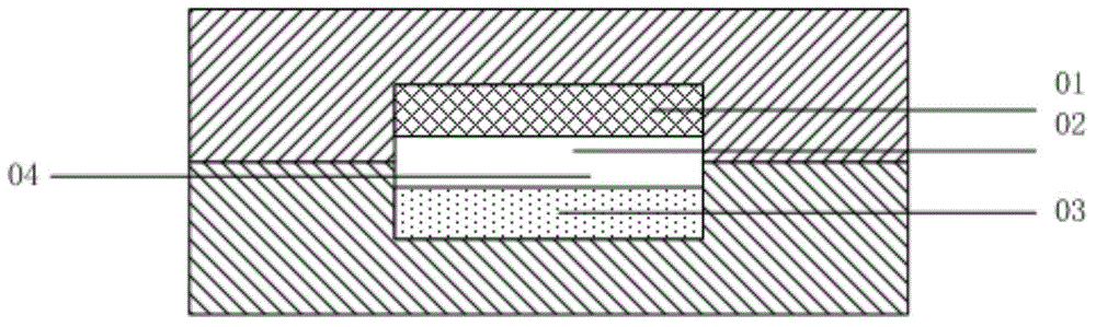
[0028] The present invention uses the traditional back-end copper interconnection technology on the surface of the wafer to be bonded to manufacture flat copper and insulators, such as a silicon dioxide insulating layer plane, and ensures one-to-one correspondence between the copper patterns on the two wafers. In the wafer hybrid bonding process, the wafer bonding is first realized, that is, the bonding between the wafer silicon dioxide insulating layer interface and the silicon dioxide insulating layer interface; secondly, the bonded wafer is placed at high temperature for annealing , due to the difference between the coefficient of thermal expansion (CTE) between the copper and the insulator, the copper with a larg...


PUM

PropertyMeasurementUnit
depthaaaaaaaaaa
depthaaaaaaaaaa

Abstract

The invention relates to a copper mixed bonding method. According to the invention, a traditional rear end copper interconnection technology is used to produce flat copper and insulator planes on the surfaces of two wafers needing to be bonded, and copper patterns on two wafers are one-to-one corresponding; in a wafer mixed bonding process, wafer bonding is completed, namely wafer insulators are bonded; the bonded wafers are placed in high temperature for annealing; copper is compressed by an insulator bonding interface, wherein the thermal expansion coefficient of copper is more than the thermal expansion coefficient of an insulator; under the combined effect of temperature and pressure, copper metal on both sides are close and are compressed and fused into a whole body, so that copper conductors on both sides are integrated into a whole body; the method is applied to the processing of machines compatible with a conventional integrated circuit; metal interconnection is realized in a mixed bonding process; and metal grains of upper and lower substrates are integrally fused, which greatly reduces cross-wafer conductor resistance and delay and provides a good process foundation for subsequent steps.

Description

technical field [0001] The invention relates to a bonding method, in particular to a copper hybrid bonding method. Background technique [0002] With the development of people's requirements for electronic products in the direction of miniaturization, multi-function, and environmental protection, people strive to make electronic systems smaller and smaller, with higher integration, more functions, and stronger . As a result, many new technologies, new materials and new designs have emerged, such as three-dimensional stacked packaging and other technologies are typical representatives of these technologies. As the development of VLSI is approaching the physical limit, 3D integrated circuits, which have advantages in both physical size and cost, are an effective way to extend Moore's Law and solve advanced packaging problems. The three-dimensional stacked packaging structure can directly stack multiple bare chips or substrates by bonding to realize the metal interconnection ...

Claims


Application Information

Patent Timeline
Patent Type & Authority Applications(China)
IPC IPC(8): H01L21/603H01L21/768
CPCH01L21/768H01L21/76898H01L24/82H01L2224/82H01L2224/828
Inventor 梅绍宁程卫华朱继锋陈俊
Owner WUHAN XINXIN SEMICON MFG CO LTD
Why Eureka
Try Eureka