Mask plate, manufacturing method of mask plate and OLED device packaging method

An encapsulation method and mask technology, which are applied to electric solid-state devices, semiconductor devices, organic semiconductor devices, etc., can solve the problems of easy breakage and poor bending resistance of the encapsulation part of flexible OLED devices, so as to ensure bending resistance. Folding effect

Active Publication Date: 2015-10-07
TCL CHINA STAR OPTOELECTRONICS TECH CO LTD
View PDF6 Cites 7 Cited by
  • Summary
  • Abstract
  • Description
  • Claims
  • Application Information

AI Technical Summary

Problems solved by technology

[0004] Because the thickness of the overall thin-film package is on the order of microns, and the stress is relatively large when the inorganic film is thick, it is easy to break when it is bent, and water and oxygen will pass through this break to age the OLED device, making the bending resistance of the flexible OLED device package part change. Difference

Method used


Image

  • Mask plate, manufacturing method of mask plate and OLED device packaging method
  • Mask plate, manufacturing method of mask plate and OLED device packaging method
  • Mask plate, manufacturing method of mask plate and OLED device packaging method

Examples


Embodiment Construction

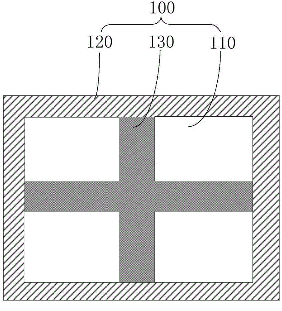
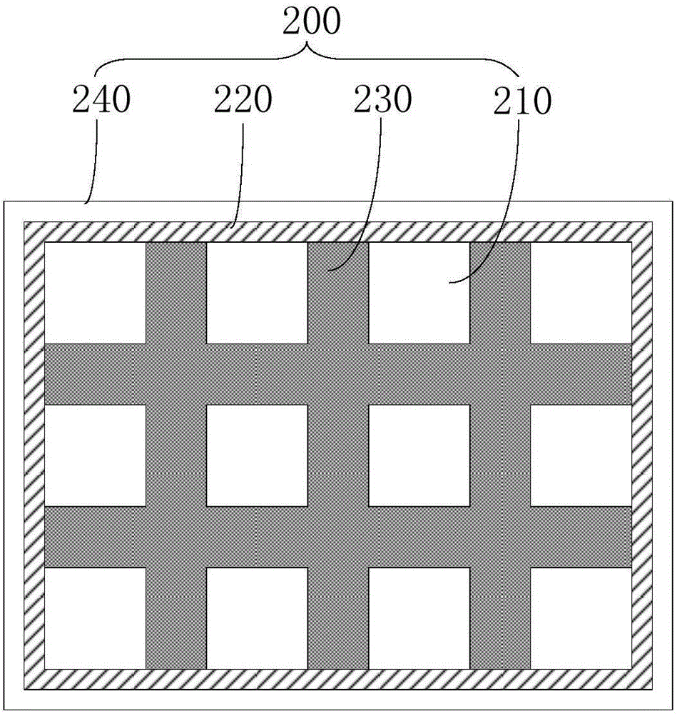
[0025] refer to figure 1 , a structural schematic diagram of the first embodiment of the mask plate of the present invention, the mask plate 100 includes a hollowed out area 110 and a non-hollowed out area 120 arranged around the hollowed out area 110; It is arranged in the hollowed out area 110 and connected to the non-hollowed out area 120 from the beginning to the end.

[0026] The hollow area 110 is a part removed by laser cutting, photolithography and etching to form a hollow shape. During coating, a large amount of coating material can pass through the hollow area 110 to form a thicker film layer.

[0027] The non-hollowed-out area 120 is the part that has not been processed. During coating, the coating material cannot pass through the non-hollowed-out area 120 and cannot form a film layer.

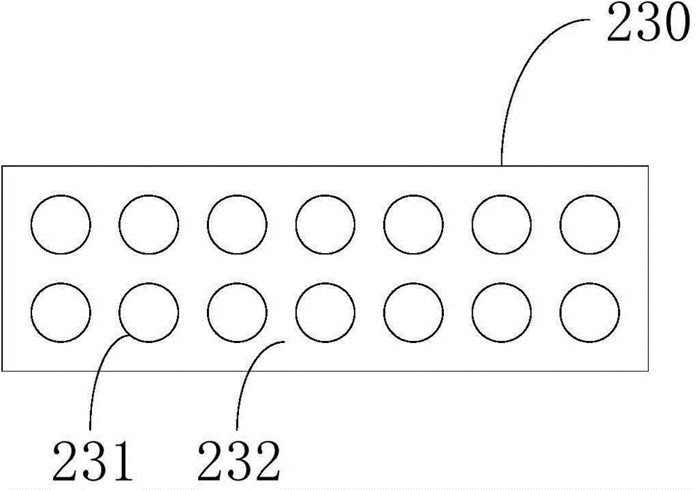
[0028] The semi-hollowed-out area 130 is a partially hollowed-out area and a partially non-hollowed-out area. During coating, a small amount of coating material can pass through th...


PUM


Abstract

The invention discloses a mask plate, a manufacturing method of the mask plate and an OLED device packaging method. The mask plate is characterized by comprising a hollowed-out area and a non-hollowed-out area arranged around the hollowed-out area. The mask plate further comprises at least one stripe-shaped semi-hollowed-out area, wherein the semi-hollowed-out area is arranged in the hollowed-out area with the head and the tail being connected with the non-hollowed-out area. Through the method disclosed by the invention, the bending performance of a packaging portion of a flexible OLED device can be strengthened.

Description

technical field [0001] The invention relates to the field of organic electroluminescence display, in particular to a mask plate, a manufacturing method thereof, and an OLED device packaging method. Background technique [0002] Organic Light-Emitting Diode (OLED), also known as Organic Light-Emitting Diode (OLED), is a new generation of display. By making an organic thin film on an OLED substrate, the organic thin film is wrapped between the cathode and anode metal, giving the two When a voltage is applied to the electrodes, the organic film will emit light. OLED displays have many advantages, including enabling flexible displays. For example, using a bendable plastic substrate as a carrier, combined with a thin film packaging process, a bendable OLED panel can be realized. [0003] At present, OLED thin-film packaging mainly adopts the structure of passivation layer and buffer layer stacking. The passivation layer is generally made of inorganic materials, such as SiNx; th...

Claims


Application Information

Patent Timeline
Patent Type & Authority Applications(China)
IPC IPC(8): H01L51/56H01L27/32C23C14/04
CPCC23C14/04C23C14/044H10K71/00H10K59/873H10K71/233H10K2102/311H10K50/844C23F1/02
Inventor 余威
Owner TCL CHINA STAR OPTOELECTRONICS TECH CO LTD
Why Eureka
Try Eureka