Transparent conductive film and capacitive touch screen containing the same
A technology of transparent conductive film and transparent substrate, applied in electrical digital data processing, input/output process of data processing, instruments, etc., can solve problems such as serious three-dimensional lines, reduce stress differences, reduce production costs, and simplify The effect of the process
- Summary
- Abstract
- Description
- Claims
- Application Information
AI Technical Summary
Problems solved by technology
Method used
Image
Examples
Embodiment 1
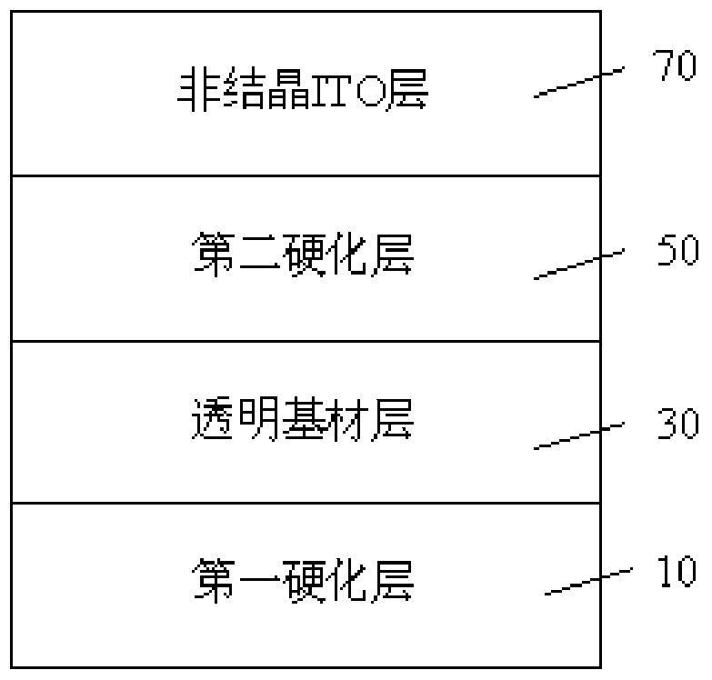
[0038] The surface of the transparent substrate layer 30 is coated with a hardening solution of the type CH202 selected from Japan Arakawa Chemical Co., Ltd., dried and cured to form the first hardened layer 10 . Then, in the same manner, the surface of the transparent substrate layer 30 far away from the first hardened layer 10 is coated with a hardening solution selected from the Japanese DIC company with a model number of PC13-1082 to form the second hardened layer 50 .
[0039] Using a magnetron sputtering process, a film is coated on the surface of the second hardened layer 50 away from the transparent substrate layer 30 to obtain an amorphous ITO layer. form figure 1 The transparent conductive film shown.
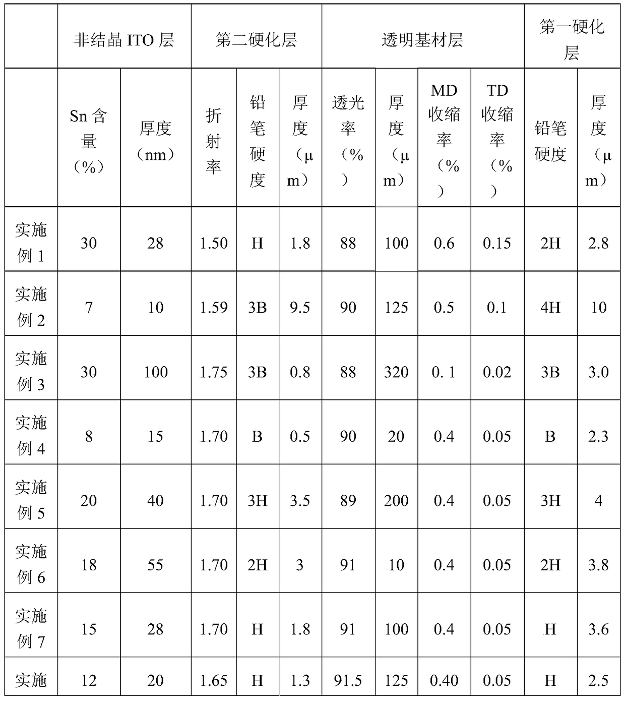
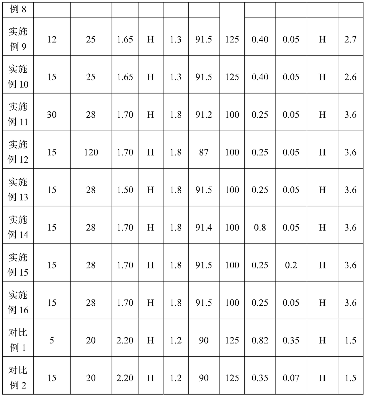
[0040] The amorphous ITO layer 70 of the transparent conductive film was etched by an ink screen printing etching method, and then baked at a temperature of 150° C. for 60 minutes. The specific structural parameters of the transparent conductive film are shown in Ta...
Embodiment 2
[0042] Adopt the same method as Example 1 to prepare a transparent conductive film, the structural parameters of the prepared transparent conductive film are shown in Table 1, wherein, the hardening solution for coating the first hardening layer 10 is the hardening solution of FZ001 from DIC Corporation of Japan, The hardening solution for coating the second hardening layer 50 is the hardening solution of JSR Corporation, Japan, whose model number is KZ6661. The specific structural parameters of the transparent conductive film are shown in Table 1.
Embodiment 3
[0044] The transparent conductive film is prepared by the same method as in Example 1. The structural parameters of the prepared transparent conductive film are shown in Table 1, wherein the hardening solution for coating the first hardening layer 10 is the hardening solution of CH202 from Japan Arakawa Chemical Co. , the hardening liquid that coats the second hardening layer 50 is the hardening liquid that the model of JSR Company of Japan is KZ6661, forms figure 1 The transparent conductive film shown. The specific structural parameters of the transparent conductive film are shown in Table 1.
PUM
| Property | Measurement | Unit |
|---|---|---|
| thickness | aaaaa | aaaaa |
| thickness | aaaaa | aaaaa |
| thickness | aaaaa | aaaaa |
Abstract
Description
Claims
Application Information
 - R&D
- Intellectual Property
- Life Sciences
- Materials
- Tech Scout
- Unparalleled Data Quality
- Higher Quality Content
- 60% Fewer Hallucinations
Browse by: Latest US Patents, China's latest patents, Technical Efficacy Thesaurus, Application Domain, Technology Topic, Popular Technical Reports.
© 2025 PatSnap. All rights reserved.Legal|Privacy policy|Modern Slavery Act Transparency Statement|Sitemap|About US| Contact US: help@patsnap.com


