Fin field effect transistor structure and manufacturing method thereof

A fin-type field effect and manufacturing method technology, which is applied in semiconductor/solid-state device manufacturing, semiconductor devices, electrical components, etc., can solve problems such as difficult control of fin width intervals and complicated process steps

Active Publication Date: 2015-09-23
SHANGHAI HUALI MICROELECTRONICS CORP
View PDF3 Cites 0 Cited by
  • Summary
  • Abstract
  • Description
  • Claims
  • Application Information

AI Technical Summary

Problems solved by technology

[0003] In the manufacturing method of the fin field effect transistor structure according to the prior art, the process steps are relatively complicated, and sometimes it is difficult to control the width of the fin and the interval between each fin

Method used


Image

  • Fin field effect transistor structure and manufacturing method thereof
  • Fin field effect transistor structure and manufacturing method thereof
  • Fin field effect transistor structure and manufacturing method thereof

Examples


Embodiment Construction

[0030] In order to make the content of the present invention clearer and easier to understand, the content of the present invention will be described in detail below in conjunction with specific embodiments and accompanying drawings.

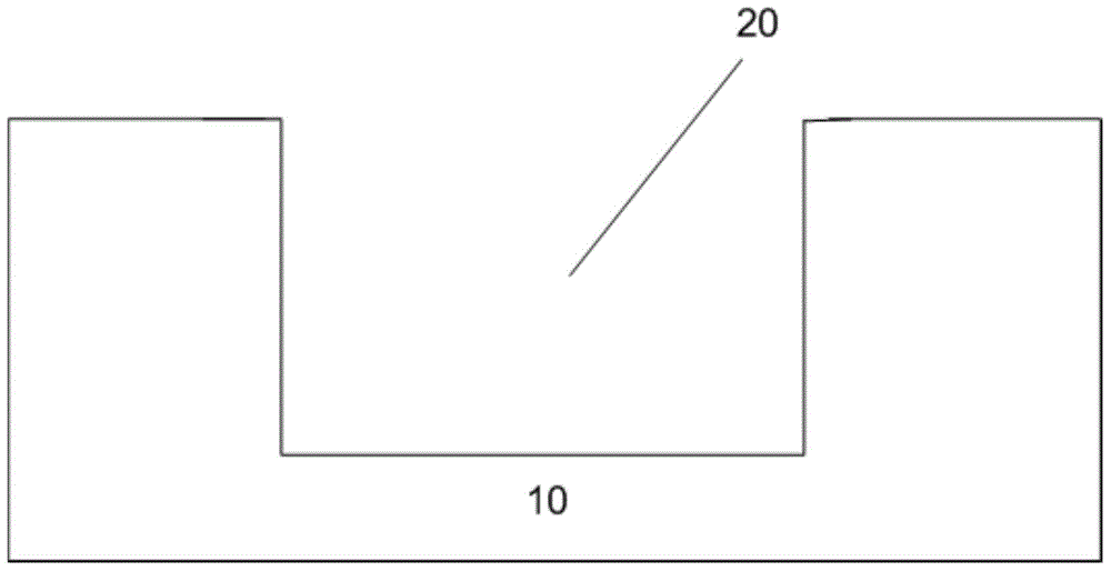
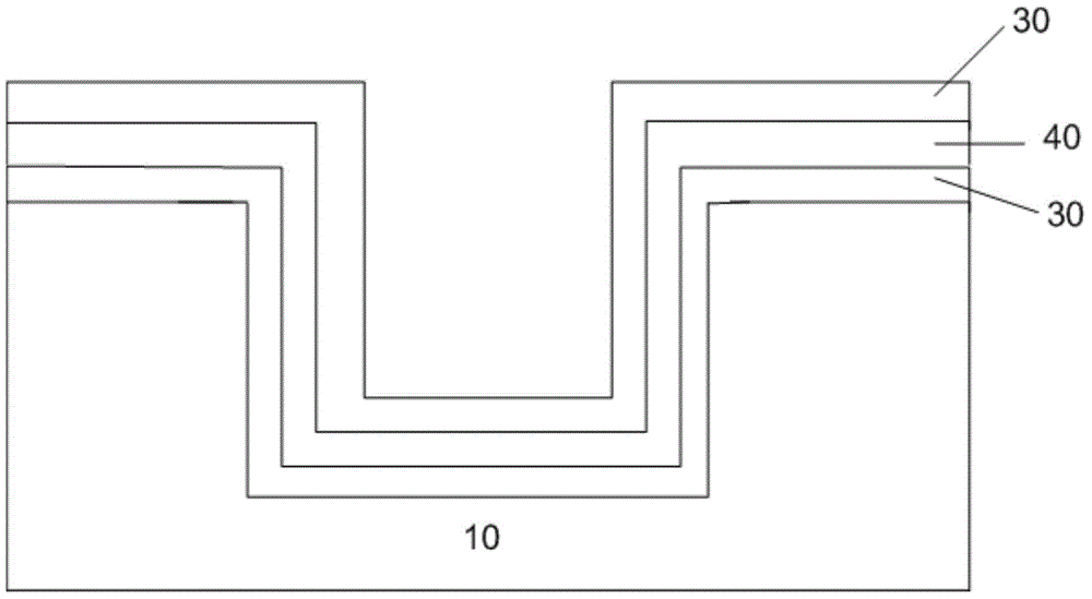
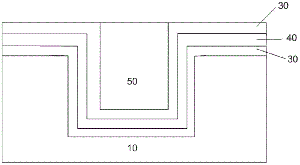
[0031] A preferred embodiment of the present invention provides a method of forming a fin structure. Among them, an initial groove is formed on the substrate by photolithography and etching, and a SiGe / Si / SiGe / ...U-type thin film stack structure is epitaxially grown in the initial groove, and a concave layer is formed in the U-shaped thin film stack structure. groove. Fill the groove with silicon oxide, and then remove excess silicon and SiGe by polishing or etching. The silicon is further etched back to form SiGe fin structures.

[0032] Of course, the epitaxial materials are preferably SiGe and Si, but the present invention is not limited to these two materials, SiGe and Si.

[0033] specifically, Figure 1 to Figure 6 Each step of the fab...


PUM


Abstract

The invention provides a fin field effect transistor structure and a manufacturing method thereof. The manufacturing method for the fin field effect transistor structure comprises the steps of: forming an initial groove in a substrate through photoetching and etching; epitaxially growing a U-shaped film laminated structure at least having a first material layer and a second material layer spaced from each other in the initial groove; filling a recessed part of the U-shaped film laminated structure with a third material; etching the third material and the silicon U-shaped film laminated structure to expose the substrate; and further etching the substrate and the second material layer to expose a fin-shaped structure formed by the first material layer.

Description

technical field [0001] The invention relates to the field of semiconductor manufacturing, and more specifically, the invention relates to a structure of a fin field effect transistor and a manufacturing method thereof. Background technique [0002] With the development of integrated circuits, the device size is getting smaller and smaller, and the integration level is getting higher and higher. Moreover, as the feature size of semiconductor devices continues to decrease due to the smaller and smaller device sizes, the traditional planar semiconductor manufacturing technology has become unusable. At present, fin field effect transistors are widely used in the field of small sizes. [0003] In the manufacturing method of the fin field effect transistor structure according to the prior art, the process steps are relatively complicated, and sometimes it is difficult to control the width of the fins and the interval between the fins. [0004] Therefore, it is desired to provide ...

Claims


Application Information

Patent Timeline
Patent Type & Authority Applications(China)
IPC IPC(8): H01L29/78H01L21/336
CPCH01L29/66477H01L29/78
Inventor 鲍宇
Owner SHANGHAI HUALI MICROELECTRONICS CORP
Why Eureka
Try Eureka