
Methods to improve FinFet semiconductor device behavior using co-implantation under the channel region

A channel region and device technology, applied in semiconductor devices, semiconductor/solid-state device manufacturing, electrical components, etc., can solve problems such as reducing short channel effects and reducing junction capacitance

Active Publication Date: 2015-09-09
GLOBALFOUNDRIES U S INC MALTA
View PDF6 Cites 10 Cited by
  • Summary
  • Abstract
  • Description
  • Claims
  • Application Information

AI Technical Summary

Problems solved by technology

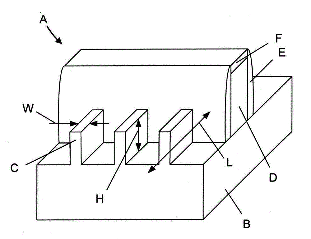
Also, within a FinFET, the junction capacitance at the drain region of the device is greatly reduced, which tends to significantly reduce short channel effects

Method used


Image

  • Methods to improve FinFet semiconductor device behavior using co-implantation under the channel region
  • Methods to improve FinFet semiconductor device behavior using co-implantation under the channel region
  • Methods to improve FinFet semiconductor device behavior using co-implantation under the channel region

Examples


Embodiment Construction

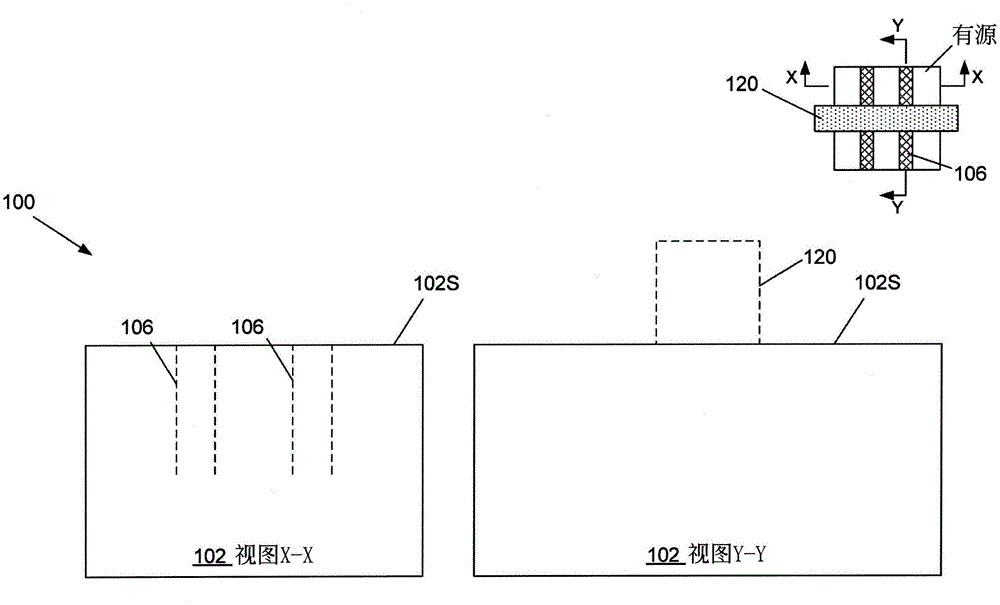
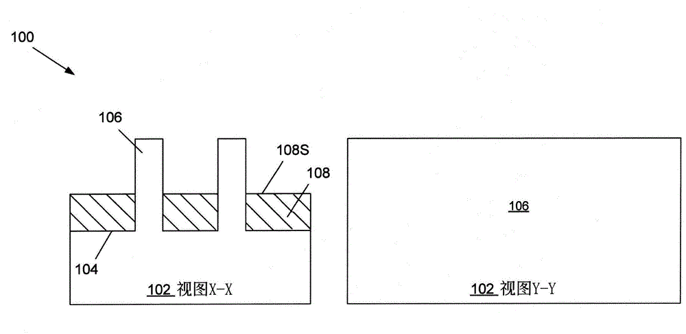
[0016] Various exemplary embodiments of the invention are described below. In the interest of clarity, not all features of an actual implementation are described in this specification. It should of course be understood that in the development of any such actual embodiment, a number of implementation-specific decisions must be made to achieve the developer's specific goals, such as the specification of system-related and business-related constraints, which will occur from one implementation to another. Variety. Furthermore, it should be appreciated that such a development effort might be complex and time-consuming, but would nevertheless be a routine undertaking within the realm of those skilled in the art having the benefit of this disclosure.

[0017]The subject matter will be explained with reference to the accompanying drawings. The exemplary depiction of various structures, systems and devices in the drawings is for purposes of explanation so as not to obscure the presen...


PUM


Abstract

One illustrative method disclosed includes, among other things, forming a fin in a substrate, forming a well implant region in at least the substrate, forming a punch-stop implant region in the fin, performing at least one neutral implantation process with at least one neutral implant material to form a neutral boron-diffusion-blocking implant region in the fin, wherein an upper surface of the neutral boron-diffusion-blocking implant region is positioned closer to an upper surface of the fin than either the punch-stop implant region or the well implant region and, after forming the well implant region, the punch-stop implant region and the neutral boron-diffusion-blocking implant region, forming a gate structure above the fin.

Description

technical field [0001] The present disclosure relates generally to the fabrication of integrated circuits and, more particularly, to various methods of forming a co-implant under a channel region of a Fin Field Effect Transistor (FinFET) semiconductor device and the resulting semiconductor device. Background technique [0002] In modern integrated circuits, eg, microprocessors, memory devices, etc., a very large number of circuit components, especially transistors, are provided and operated on a restricted chip area. In integrated circuit fabrication using metal-oxide-semiconductor (MOS) technology, field effect transistors (FETs), including NMOS and PMOS transistors, are provided, usually operating in a switch mode. That is, these transistor devices exhibit a highly conductive state (on-state) as well as a high impedance state (off-state). FETs can take various forms and configurations. For example, in other configurations the FETs may be so-called planar FET devices or t...

Claims


Application Information

Patent Timeline
Patent Type & Authority Applications(China)
IPC IPC(8): H01L21/265H01L21/336
CPCH01L29/66795H01L21/265H01L29/0638H01L29/7851H01L21/26506H01L29/1083
Inventor M·乔希J·M·范梅尔M·埃勒
Owner GLOBALFOUNDRIES U S INC MALTA
Learn More