Display device and electronic apparatus
A technology for display devices and potentials, applied to static indicators, instruments, etc., can solve the problems of high cost of display devices
- Summary
- Abstract
- Description
- Claims
- Application Information
AI Technical Summary
Problems solved by technology
Method used
Image
Examples
no. 1 Embodiment approach
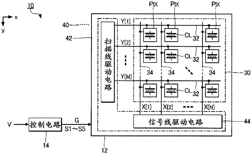
[0048] figure 1 It is a block diagram of the display device 10 according to the first embodiment of the present invention. The display device 10 is an electronic device that displays a planar image, and includes an electro-optic panel 12 and a control circuit 14 .
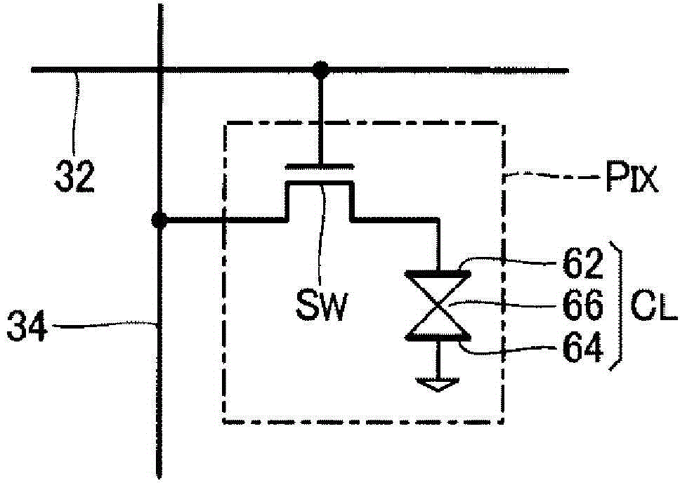
[0049] The electro-optical panel 12 includes a pixel portion 30 in which a plurality of pixels (pixel circuits) PIX are arranged, and a drive circuit 40 for driving each pixel PIX. In the pixel portion 30 , M scanning lines 32 extending in the x direction and N signal lines 34 extending in the y direction intersecting the x direction are formed (M and N are natural numbers). A plurality of pixels PIX in the pixel unit 30 are arranged in a matrix of M rows in the vertical direction and N columns in the horizontal direction corresponding to intersections of the scanning lines 32 and the signal lines 34 . In this embodiment, the pixels PIX are arranged at all of the M×N intersections formed by the M scanning lines 3...
no. 2 Embodiment approach
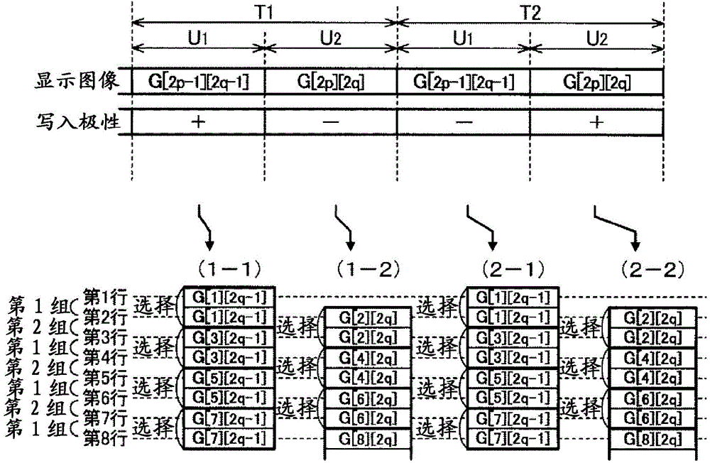
[0156] In the first embodiment, the block BL(2p-1)(2q-1) selected in the unit period U1 is such that the block BL(2p)(2q) selected in the unit period U2 is positioned in the vertical direction (x direction) and y direction) are displaced by 1 pixel each.
[0157] On the other hand, in the second embodiment, the block BL selected in the unit period U1 is a point in which the block BL selected in the unit period U2 is shifted by one pixel in the vertical direction (y direction). 1 The implementations are different.
[0158] As follows, while referring to Figure 11 and Figure 12 , the display device 10 according to the second embodiment will be described. In addition, as for elements having the same action and / or function as those of the first embodiment in each of the embodiments exemplified below, the symbols referred to in the above description are used, and detailed descriptions of each are appropriately omitted.
[0159] as shown in Figure 11 In the part (1-1) and pa...
Deformed example 1
[0168] In the display device 10 according to the first embodiment described above, in the unit period U1, each of the plurality of pixels PIX located in odd-numbered rows and odd-numbered columns is used as a reference pixel, and a plurality of blocks corresponding to each of the plurality of reference pixels are specified. BL, and in the unit period U2, each of a plurality of pixels PIX located in an even row and an even column is used as a reference pixel, and a plurality of blocks BL corresponding to the plurality of reference pixels are designated, but the present invention is not limited to such Alternatively, in the unit period U1, each of the plurality of pixels PIX located in an even row and an even column may be used as a reference pixel, and a plurality of blocks BL corresponding to the plurality of reference pixels may be designated, and in the unit period U2, Using each of the plurality of pixels PIX located in odd-numbered rows and odd-numbered columns as a referen...
PUM
 Abstract
Description
Claims
Application Information
 - R&D
- Intellectual Property
- Life Sciences
- Materials
- Tech Scout
- Unparalleled Data Quality
- Higher Quality Content
- 60% Fewer Hallucinations
Browse by: Latest US Patents, China's latest patents, Technical Efficacy Thesaurus, Application Domain, Technology Topic, Popular Technical Reports.
© 2025 PatSnap. All rights reserved.Legal|Privacy policy|Modern Slavery Act Transparency Statement|Sitemap|About US| Contact US: help@patsnap.com


