Array substrate, display panel, and manufacturing method of array substrate

A technology of array substrate and substrate substrate, which is applied in semiconductor/solid-state device manufacturing, instruments, semiconductor devices, etc., can solve problems such as signal breakage, copper surface bombardment, and transparent electrode oxidation and corrosion, and achieves improved reliability and low production cost. Effect

Active Publication Date: 2015-09-02
HEFEI XINSHENG OPTOELECTRONICS TECH CO LTD +1
View PDF3 Cites 5 Cited by
  • Summary
  • Abstract
  • Description
  • Claims
  • Application Information

AI Technical Summary

Problems solved by technology

[0006] In the manufacturing process of the array substrate using copper as the gate metal in the prior art, because copper is highly active and easy to oxidize, when making the first insulating layer above the gate metal, a high temperature of more than 300°C is often required , after the temperature rises, the copper surface is easily oxidized; after the passivation layer is deposited, a high-power plasma is used for dry etching, which will further bombard the copper surface; and the gate metal and transparent electrode There is high-temperature annealing in the manufacturing process after contact, and high-temperature annealing will easily cause the transparent electrode on the edge of the via hole to be oxidized and corroded, resulting in signal breakage

Method used


Image

  • Array substrate, display panel, and manufacturing method of array substrate
  • Array substrate, display panel, and manufacturing method of array substrate
  • Array substrate, display panel, and manufacturing method of array substrate

Examples


Embodiment Construction

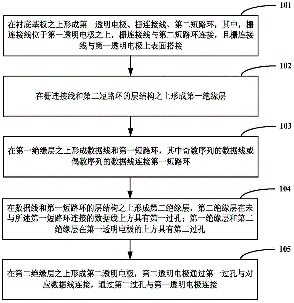
[0050] In order to improve the reliability of signal transmission at a via hole connected to a short-circuit ring on an array substrate, an embodiment of the present invention provides an array substrate, a display panel, and a method for manufacturing the array substrate. In order to make the purpose, technical solution and advantages of the present invention clearer, the following examples are given to further describe the present invention in detail.

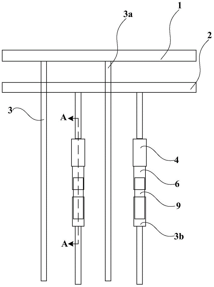
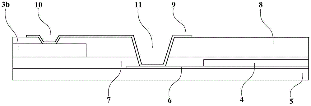
[0051] like figure 1 and figure 2As shown, the array substrate provided by the embodiment of the present invention includes a set of data lines 3 and a set of gate lines arranged crosswise, and a first short-circuit ring 1 and a second short-circuit ring 2 located in the peripheral area of ​​the array substrate. The first short-circuit ring 1 is set on the same layer as a group of data lines 3, and the second short-circuit ring 2 is set on the same layer as a group of gate lines; in a set of data lines 3, two adjacent data ...


PUM


Abstract

The invention discloses an array substrate, a display panel, and a manufacturing method of an array substrate. Therefore, signal transmission reliability at the via hole for connecting short-circuit rings of the array substrate can be improved. The array substrate comprises a group of data lines, a group of grid lines, a first short-circuit ring, and a second short-circuit ring, wherein the first short-circuit ring and the second short-circuit ring are arranged at the peripheral area of the array substrate. The first short-circuit ring and the group of data lines are arranged at the same layer; and the second short-circuit ring and the group of grid lines are arranged at the same layer. Each two adjacent data lines are respectively connected with the first short-circuit ring and the second short-circuit ring. The connection structure of the second short-circuit ring and the data line includes a first transparent electrode arranged on the substrate, a grid connection line arranged on the first transparent electrode, and a first insulation layer arranged on the first transparent electrode and the grid connecting line; a second insulation layer arranged on the data line, and a second transparent electrode arranged on the second insulation layer; and the data line is arranged on the first insulation layer.

Description

technical field [0001] The present invention relates to the field of display technology, in particular to an array substrate, a display panel and a method for manufacturing the array substrate. Background technique [0002] Among flat panel display devices, Thin Film Transistor Liquid Crystal Display (TFT-LCD for short) has the characteristics of small size, low power consumption, relatively low manufacturing cost and no radiation, and occupies a dominant position in the current flat panel display market. leading position. [0003] At present, the display modes of TFT-LCD mainly include TN (Twisted Nematic, twisted nematic) mode, VA (Vertical Alignment, vertical orientation) mode, IPS (In-Plane-Switching, plane direction conversion) mode and AD-SDS (ADvanced Super Dimension Switch, advanced ultra-dimensional field switching technology, referred to as ADS) mode, etc. [0004] Among them, the ADS mode has been developed to 0+4 patterning process, and its advantage is that th...

Claims


Application Information

Patent Timeline
Patent Type & Authority Applications(China)
IPC IPC(8): H01L27/12H01L27/32H01L21/77
CPCG02F1/1362H01L27/124G02F1/136254H01L27/1244G02F1/136286G02F1/133345G02F1/13439G02F1/136227H01L27/1288G02F1/136295
Inventor 蔡振飞方娟魏晓梅陈敏
Owner HEFEI XINSHENG OPTOELECTRONICS TECH CO LTD
Why Eureka
Try Eureka