
Pixel arrangement structure, organic electroluminescent device, display device, and mask plate

A pixel arrangement, pixel technology, applied in the direction of electric solid devices, electrical components, semiconductor devices, etc., can solve the problems of screen color mixing, the size of the opening area is reduced, and the light-emitting area is small, and the screen display is clear and high-resolution. the effect of increasing the luminous area

Inactive Publication Date: 2015-08-12
BOE TECH GRP CO LTD +1
View PDF4 Cites 34 Cited by
  • Summary
  • Abstract
  • Description
  • Claims
  • Application Information

AI Technical Summary

Problems solved by technology

For high-resolution AMOLED, Fine Metal Mask (FMM) is one of the most critical technologies restricting its development. It is becoming more and more difficult. At the same time, due to the improvement of resolution, the distance between the sub-pixel light-emitting areas is required to be smaller and smaller, and the color mixing of the evaporated screen will become more and more serious, especially the traditional red and green stripes. , blue (R, G, B) three sub-pixels, each sub-pixel corresponds to the length of the opening area of ​​the FMM is long, linearity control is difficult, and color mixing is prone to occur
Although the traditional RGB arrangement of dots (Slots) does not lead to a longer opening ratio and length, and the linearity is difficult to control, in the process of making the opening area of ​​FMM, there must be a gap between the opening areas of each Slot. There is a certain metal raw material as a connecting bridge (called Rib), which leads to a reduction in the size of the sub-pixel FMM opening area, thereby affecting the aperture ratio of the OLED display device
The aperture ratio is low, and the brightness and life cannot meet the requirements
As a result, the yield rate of AMOLED products is low, which limits the mass production of high-resolution AMOLED panels
Therefore, a pentile pixel arrangement method is proposed in the prior art, but this arrangement method has problems such as aggravated image crosstalk and deterioration of oblique line aliasing.
[0005] To sum up, the pixel arrangement structure in the prior art cannot avoid the problem of the small opening area of ​​the metal mask on the premise of ensuring no crosstalk in the image, thus resulting in a small light-emitting area and a low opening ratio. The brightness and lifespan cannot meet the requirements, which makes the yield rate of AMOLED products low and limits the mass production of high-resolution AMOLED panels

Method used


Image

  • Pixel arrangement structure, organic electroluminescent device, display device, and mask plate
  • Pixel arrangement structure, organic electroluminescent device, display device, and mask plate
  • Pixel arrangement structure, organic electroluminescent device, display device, and mask plate

Examples


Embodiment Construction

[0028] An embodiment of the present invention provides a pixel arrangement structure, an organic electroluminescent device, a display device, and a mask, which are used to make the opening area of ​​the metal mask for manufacturing the pixel arrangement structure larger, thereby increasing the aperture ratio and improving AMOLED products. Brightness, longevity, and picture quality clarity.

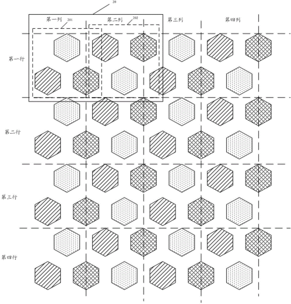
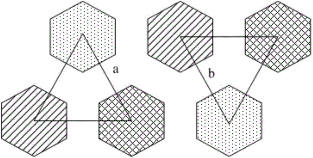
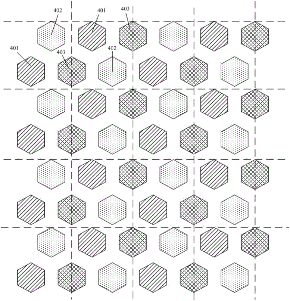
[0029] A pixel arrangement structure provided by an embodiment of the present invention includes a plurality of pixels composed of three sub-pixels of different colors, wherein the connecting lines between the center points of each sub-pixel form an equilateral triangle, so that these sub-pixels are arranged in a dot-like dislocation , the shape of each sub-pixel is a polygon with sides greater than four, such as a pentagon or a hexagon, and the hexagon or pentagon has a larger light-emitting area than a quadrangle, effectively utilizing the light-emitting area, making The area that emits ...


PUM


Abstract

The present invention discloses a pixel arrangement structure, an organic electroluminescent device, a display device, and a mask plate such that the opening area of a metal mask plate for manufacturing the pixel arrangement structure is large, thus the aperture ratio is raised, and the AMOLED product brightness, service life and picture quality sharpness are improved. The pixel arrangement structure provided by the invention comprises a pixel formed by three sub pixels with different colors, an equilateral triangle is formed by the center point connection lines of the sub pixels, and the shape of each sub pixel is a polygon with more than four sides.

Description

technical field [0001] The invention relates to the technical field of displays, in particular to a pixel arrangement structure, an organic electroluminescence device, a display device, and a mask plate. Background technique [0002] In mobile phone and tablet display technologies, Active Matrix Organic Light Emitting Diode (AMOLED) panels will gradually become the mainstream of next-generation displays due to their advantages such as self-illumination, bright colors, low power consumption, and wide viewing angles. [0003] The principle of AMOLED self-luminescence includes: use the indium tin oxide semiconductor (ITO) electrode and the metal electrode made on the backplane as the anode and cathode of the device respectively, vapor-deposit the organic semiconductor material and the luminescent material on the substrate, and drive it at a certain voltage Next, electrons and holes are injected from the cathode and anode into the electron and hole transport layers respectively,...

Claims


Application Information

Patent Timeline
IPC IPC(8): H01L27/32H01L51/56
CPCH10K59/121H10K71/10H10K59/353H10K50/80H10K59/122
Inventor 嵇凤丽梁逸南白珊珊玄明花孙亮
Owner BOE TECH GRP CO LTD
Learn More