a d flip flop

A flip-flop and inverter technology, applied in the direction of pulse generation, electrical components, generating electrical pulses, etc., can solve problems affecting subsequent operations, system errors or crashes, etc.

Active Publication Date: 2017-09-15
NO 47 INST OF CHINA ELECTRONICS TECH GRP
View PDF5 Cites 0 Cited by
  • Summary
  • Abstract
  • Description
  • Claims
  • Application Information

AI Technical Summary

Problems solved by technology

D flip-flop is the most widely used sequential device in integrated circuits. This device will retain the error information after the occurrence of single-event reversal and single-event transient pulse, which will affect the subsequent operation, resulting in the error or collapse of the entire system, resulting in serious consequence

Method used


Image

  • a d flip flop
  • a d flip flop
  • a d flip flop

Examples


Embodiment Construction

[0025] Below in conjunction with accompanying drawing, invention is described in further detail.

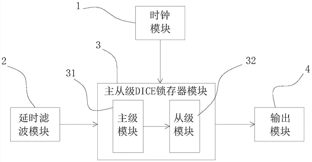
[0026] Such as figure 1 As shown, the D flip-flop in an embodiment of the present invention includes a clock module 1 , a delay filter module 2 , a master-slave DICE latch module 3 , and an output module 4 . The master-slave DICE latch module 3 includes a master module 31 and a slave module 32, both master-slave stages are reinforced with DICE, and a delay filter module 2 is added at the data end.

[0027] The clock signal output of the clock module 1 is connected to the clock signal input of the master-slave DICE latch module 3, the data input of the delay filter module 2 is connected to the data source, and the data output is connected to the master-slave DICE latch The data input end of the module 3 is connected, and the data output end of the master-slave DICE latch module 3 is connected to the signal input end of the output module 4 .

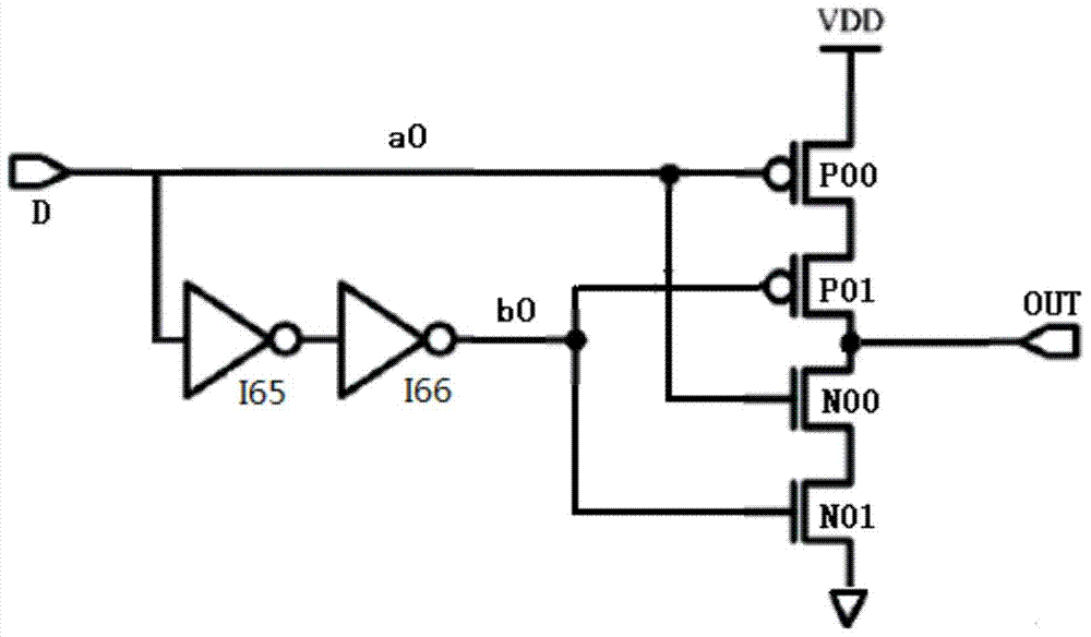
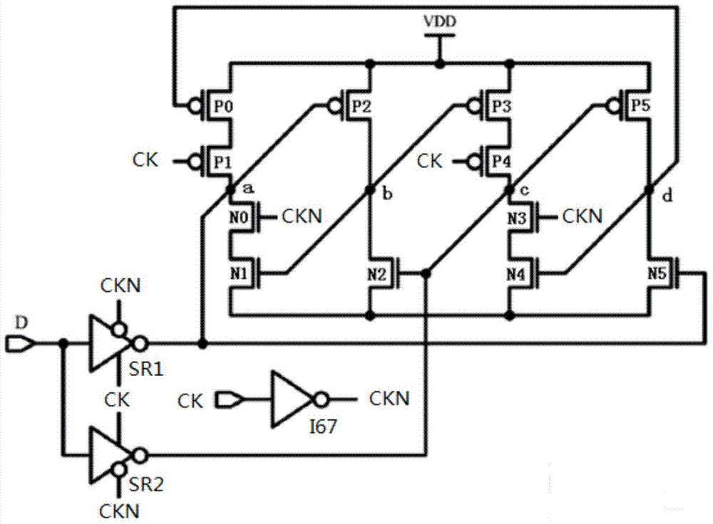
[0028] figure 2 A schematic diagra...


PUM


Abstract

A D flip-flop, comprising a clock module, a delay filter module, a master-slave DICE latch module, an output module, wherein the master-slave DICE latch module is based on the clock signal output from the clock module, and through the The external data signal received by the delay filter module is output to the data output module corresponding to the data signal. The master-slave DICE latch module consists of a master module and a slave module. The delay filter module is used to prevent the transient pulse caused by the single event effect from entering the register. The master-slave DICE latch module is used to correct the internal node flipping caused by the single event effect; the delay filter module plays the role of anti-single event transient pulse, and the master-slave DICE latch module prevents the internal storage node from flipping , to play the role of anti-single event flipping, adding a guard band structure in the layout design, which effectively suppresses single-event latch-up, and also helps to reduce the single-event transient pulse width in the circuit.

Description

technical field [0001] The invention relates to the field of semiconductor devices, in particular to a D flip-flop. Background technique [0002] When a semiconductor device is in a radiation environment, the surrounding energy particles will penetrate into the chip and generate ionizing radiation, which will generate a certain number of electron and hole pairs on the trajectory of the energy particles. These electrons and holes generated by the ionizing radiation of single energy particles may be absorbed by the internal nodes of the circuit under the action of the electric field, resulting in abnormal function of the semiconductor device. These effects are called single event effects. [0003] A single event effect is a random effect. In 1975, people discovered the abnormal flip phenomenon of Binder, communication satellites, and JK triggers. After continuous research, it was found that the factors that caused the abnormal flip phenomenon included high-energy protons, he...

Claims


Application Information

Patent Timeline
Patent Type & Authority Patents(China)
IPC IPC(8): H03K3/3562
Inventor 陈智王爽
Owner NO 47 INST OF CHINA ELECTRONICS TECH GRP
Why Eureka
Try Eureka