
An organic electroluminescence display panel and a display device

An electroluminescence display and display panel technology, applied in static indicators, instruments, etc., can solve the problems of unfavorable high-resolution display panel production, increase of display panel wiring, increase of driver chip area, etc., so as to reduce the driver chip area , reduce the number of signal channels, improve the effect of uniformity

Active Publication Date: 2016-05-11
BOE TECH GRP CO LTD
View PDF8 Cites 3 Cited by
  • Summary
  • Abstract
  • Description
  • Claims
  • Application Information

AI Technical Summary

Problems solved by technology

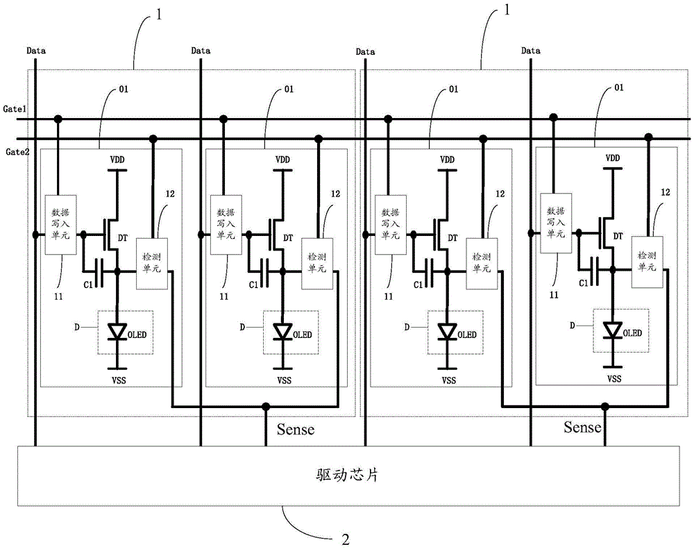
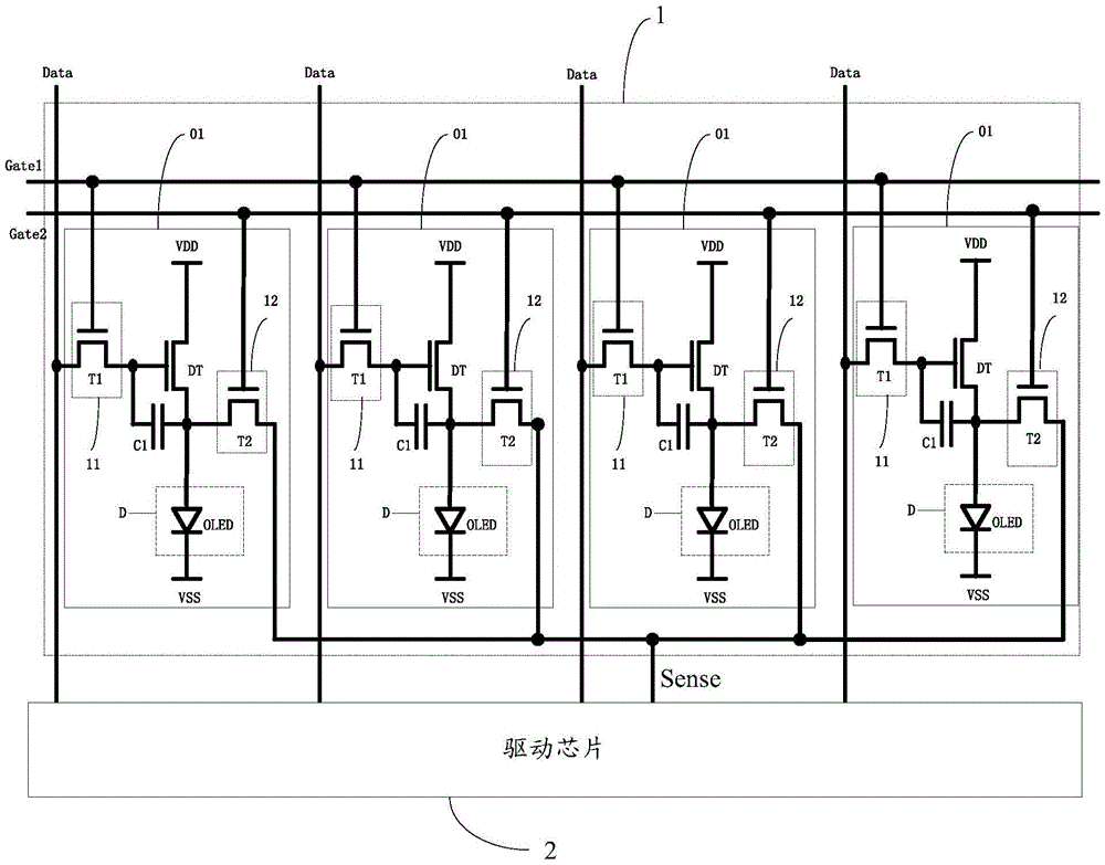
However, in the above-mentioned display panel, since each sub-pixel is connected with a sense line, the wiring in the display panel increases, which is not conducive to the manufacture of a high-resolution display panel, and the number of signal channels of the driving chip will also be doubled. Causes the area of ​​the driver chip to increase and the cost to increase

Method used


Image

  • An organic electroluminescence display panel and a display device
  • An organic electroluminescence display panel and a display device
  • An organic electroluminescence display panel and a display device

Examples


Embodiment Construction

[0036] In order to clearly illustrate the solutions of the embodiments of the present invention, the principles of the embodiments of the present invention will be firstly described below.

[0037] For the light-emitting device in each sub-pixel, its luminous efficiency decreases continuously with the aging of time. Different light-emitting devices, with the same initial luminous efficiency, have different degrees of reduction in luminous efficiency over time. However, after obtaining the aging conditions of each light emitting device, the initial grayscale value of the corresponding sub-pixel is compensated according to the aging conditions of the light emitting device in each sub-pixel, so that the actual luminous brightness of the light emitting device is the same as that of the light emitting device at Under the initial luminous efficiency, the luminous brightness is the same when the gray scale input to the sub-pixel is the above initial gray scale value.

[0038] For an ...


PUM


Abstract

The invention discloses an organic electroluminescence display panel and a display device. A data writing unit is used to write a first preset voltage to the gate of a drive transistor, a detection unit is used to receive the drive current of the drive transistor, and the detection line is used to calculate the voltage. drive the current, and adjust the gate voltage of the drive transistor until the amount of change in the voltage on the detection line is a preset value, thereby calculating the change amount of the drive voltage of the light emitting device by calculating the change amount of the gate voltage of the drive transistor, and then The obtained corresponding aging condition of the light-emitting device. Then, the initial gray scale value of the corresponding sub-pixel is compensated according to the aging condition of the light-emitting device in each sub-pixel, thereby improving the uniformity of the brightness of the display panel. In addition, multiple sub-pixels belonging to the same pixel group in the display panel share one detection line, which can reduce the number of wiring in the display panel, thereby reducing the number of signal channels of the driving chip and reducing the area of ​​the driving chip to reduce production costs.

Description

technical field [0001] The invention relates to the field of display technology, in particular to an organic electroluminescent display panel and a display device. Background technique [0002] Organic Light Emitting Diode (OLED), as a current-mode light-emitting device, has been increasingly used in high-performance displays. Traditional passive matrix organic light emitting diode (PassiveMatrixOLED, PMOLED) displays require a shorter driving time of a single pixel as the display size increases, and thus need to increase transient current and increase power consumption. At the same time, the application of high current will cause the voltage drop on the ITO line to be too large, and the working voltage of the OLED will be too high, thereby reducing its efficiency. The active matrix organic light-emitting diode (ActiveMatrixOLED, AMOLED) display input OLED current through the progressive scan of the switch tube, which can well solve these problems. [0003] Among the three...

Claims


Application Information

Patent Timeline
Patent Type & Authority Patents(China)
IPC IPC(8): G09G3/3275
CPCG09G3/3233G09G2300/0426G09G2300/0465G09G2300/0842G09G2320/0295G09G2300/0819G09G2320/0233G09G2320/045G09G3/3241G09G3/3291G09G2320/048G09G2330/12
Inventor 宋丹娜
Owner BOE TECH GRP CO LTD
Learn More