Display substrate, display panel, display device, and method for manufacturing display substrate

A technology for display substrates and substrate substrates, applied in nonlinear optics, instruments, optics, etc., can solve problems such as the inability to integrate display panels and light sources, achieve the effect of reducing optical difference, avoiding influence, and improving integration

Inactive Publication Date: 2017-11-14
BOE TECH GRP CO LTD +1
View PDF6 Cites 0 Cited by
  • Summary
  • Abstract
  • Description
  • Claims
  • Application Information

AI Technical Summary

Problems solved by technology

[0005] The object of the present invention is to provide a display substrate, a display panel, a display device, and a method for manufacturing a display substrate, which can integrate a backlight on the substrate, thereby achieving the technical effect of integrating the backlight and the substrate, and solving the problem of display problems in the display device. The problem that the panel and the light source cannot be integrated

Method used


Image

  • Display substrate, display panel, display device, and method for manufacturing display substrate
  • Display substrate, display panel, display device, and method for manufacturing display substrate
  • Display substrate, display panel, display device, and method for manufacturing display substrate

Examples


Embodiment 1

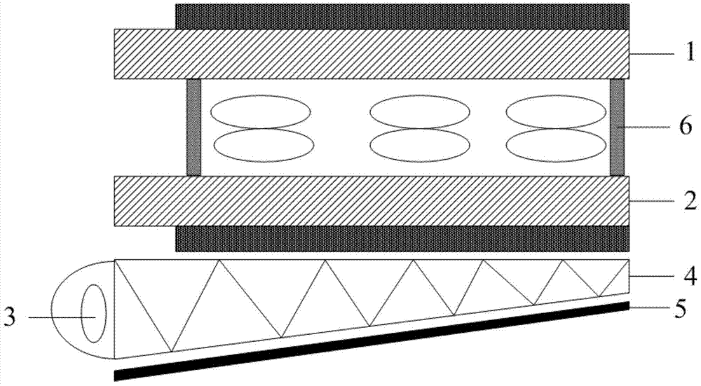
[0078] In the first embodiment provided by the present invention, the display substrate is a color filter substrate.

[0079] image 3 Shown is a schematic structural view of the display substrate provided in this embodiment as a color filter substrate, wherein some structures not related to the present invention are not shown in the figure.

[0080] Figure 4 Shown is a schematic structural view of a display device using the display substrate provided in this embodiment as a color filter substrate, wherein some structures not related to the present invention are not shown in the figure.

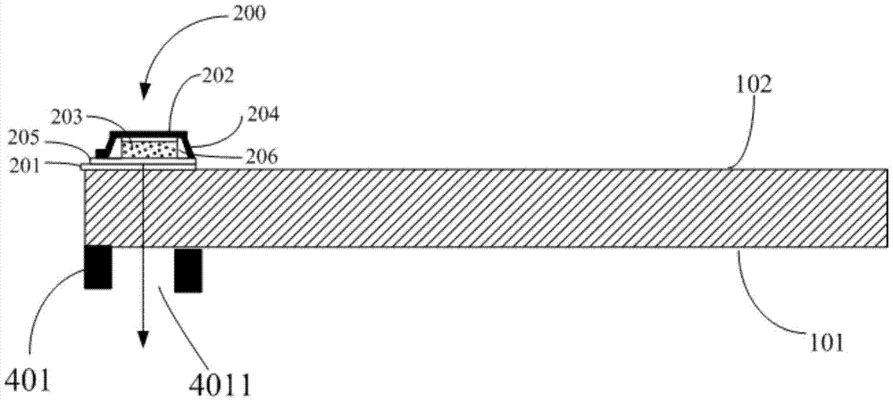
[0081] like image 3 and Figure 4 As shown, when the display substrate is a color filter substrate, the base substrate includes opposite first surfaces 101 and second surfaces 102; wherein, the display area of ​​the first surface 101 of the base substrate is provided with A black matrix (not shown in the figure), the light source structure 200 is arranged in the peripheral area of ​​the...

Embodiment 2

[0106] In the second embodiment provided by the present invention, the display substrate is an array substrate.

[0107] Figure 5 Shown is a schematic structural view of the display substrate provided in this embodiment as an array substrate, and some structures not related to the present invention are not shown in the figure.

[0108] Image 6 Shown is a schematic structural view of a display panel using the display substrate provided in this embodiment as an array substrate, and some structures not related to the present invention are not shown in the figure.

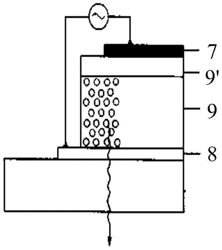
[0109] like Figure 5 and Image 6 As shown, when the display substrate is an array substrate 20, the base substrate includes opposite third surfaces 103 and fourth surfaces 104; wherein, the display area of ​​the third surface 103 is provided with thin film transistors (not shown ), the peripheral area of ​​the fourth surface 104 of the base substrate is provided with the light source structure 200, and the ligh...


PUM


Abstract

The invention provides a display substrate, a display panel, a display device and a manufacturing method of the display substrate. The display substrate comprises a substrate body, a light source structure and a light shading structure, wherein the substrate body comprises a display area and a peripheral area, the light source structure is formed on the peripheral area of the substrate body, and the light shading structure is used for limiting the light emitting direction of light emitted by the light source structure so that the light source structure can emit in the preset direction. According to the scheme, backlight integration can be performed on the display substrate, so that the technical effect of integrating backlight and the display substrate is achieved, and the problem that a display panel of an existing display device and a light source cannot be integrated is solved.

Description

technical field [0001] The present invention relates to the field of display technology, in particular to a display substrate, a display panel, a display device and a method for manufacturing the display substrate. Background technique [0002] figure 1 Shown is a schematic structural diagram of a current TFT-LCD (Thin Film Transistor—Liquid Crystal Display, liquid crystal display). like figure 1 As shown, the current TFT-LCD includes a display panel and a backlight module, in which the display panel is formed by a color filter substrate (CF) 1 and an array substrate (TFT) 2 through a pair of sealing glue 6, and the backlight module mainly includes a frame , light source 3, light guide plate 4, bottom reflector 5, and optical film, etc., wherein the light guide plate 4 is generally arranged below the array substrate 2, the light source 3 is arranged on the frame, and is located on one side of the light guide plate 4, and the light emitted by the light source The light ent...

Claims


Application Information

Patent Timeline
Patent Type & Authority Patents(China)
IPC IPC(8): G02F1/13357G02F1/1333
CPCG02F1/1335G02F1/133512G02F1/1336
Inventor 曲连杰郭建
Owner BOE TECH GRP CO LTD
Why Eureka
Try Eureka