
Manufacturing method of black matrix

A technology of black matrix and production method, which is applied in the field of production of black matrix, and can solve problems such as difficult identification of alignment marks

Active Publication Date: 2015-07-08
SHENZHEN CHINA STAR OPTOELECTRONICS TECH CO LTD
View PDF5 Cites 11 Cited by
  • Summary
  • Abstract
  • Description
  • Claims
  • Application Information

AI Technical Summary

Problems solved by technology

[0008] The purpose of the present invention is to provide a method for making a black matrix, which solves the problem that the alignment marks are difficult to identify during the preparation of the black matrix in the BOA structure

Method used


Image

  • Manufacturing method of black matrix
  • Manufacturing method of black matrix
  • Manufacturing method of black matrix

Examples


Embodiment Construction

[0037] In order to further illustrate the technical means adopted by the present invention and its effects, the following describes in detail in conjunction with preferred embodiments of the present invention and accompanying drawings.

[0038] see Figure 4 , the invention provides a kind of manufacture method of black matrix, comprises the steps:

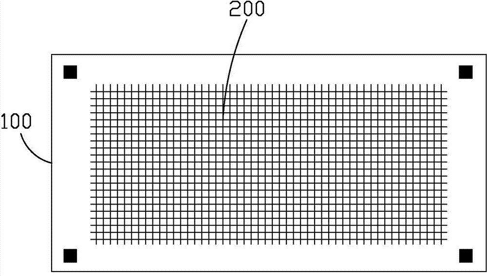
[0039] Step 1. Please refer to Figure 5 , a substrate 1 is provided, and several alignment marks 14 are arranged on the substrate 1 .

[0040] Preferably, the substrate 1 has a rectangular structure, and the alignment marks 14 are four, which are respectively arranged at four corners of the rectangle.

[0041] Specifically, the substrate 1 is a TFT array substrate.

[0042] Step 2, see Figure 6-7 , providing a black matrix photoresist system, and coating the black matrix photoresist system on the substrate 1 to form a photoresist layer 2 , the photoresist layer 2 covers the entire substrate 1 and the alignment marks 14 on th...


PUM


Abstract

The invention provides a manufacturing method of a black matrix. A black matrix light resistance system which comprises negative photoresist and metal halide is arranged on a substrate in a coating mode, a light resistance layer is formed, the metal halide is materials with low optical density values when exposure is not carried out, so that the light resistance layer is in a transparent state, and identification on marks is convenient. After exposure, the metal halide can be decomposed into metal particles, the metal particles appear to be black due to the size is small, so that the light resistance layer appears to be black, accordingly, the light blocking function of the black matrix is achieved, and the feature that the negative photoresist can be dissolved in developing liquid when exposure is not carried out, and after exposure, the negative photoresist cannot be dissolved in the developing liquid is used for solving the problem that during a BOA manufacturing process, after black matrix light resistance system coating, counterpoint marks cannot be recognized easily.

Description

technical field [0001] The invention relates to the field of display technology, in particular to a method for manufacturing a black matrix. Background technique [0002] With the development of display technology, liquid crystal displays (Liquid Crystal Display, LCD) and other flat display devices are widely used in mobile phones, televisions, personal Various consumer electronic products such as digital assistants, digital cameras, notebook computers, and desktop computers have become the mainstream of display devices. [0003] Most of the liquid crystal display devices currently on the market are backlight liquid crystal displays, which include a liquid crystal display panel and a backlight module. The working principle of the liquid crystal display panel is to place liquid crystal molecules between two parallel glass substrates. There are many vertical and horizontal small wires between the two glass substrates. The direction of the liquid crystal molecules is controlle...

Claims


Application Information

Patent Timeline
IPC IPC(8): G02F1/1335G03F7/00
CPCG02F1/1303G02F1/136209G03F7/00
Inventor 熊源
Owner SHENZHEN CHINA STAR OPTOELECTRONICS TECH CO LTD
Learn More