


Quick Research
Generate reliable direction feasibility study reports for your R&D in just a few steps.

Technical Q&A
Discover and master advanced knowledge NOW. Basics, ideas, possibilities, all at once.

Find Solutions
As an expert in R&D theories, this can generate solutions to your technical problems instantly.

Evaluate Feasibility
Analyze your overall solution with one click, know your potential R&D risks in advance.

Monitor Landscape
Get weekly tech updates, stay abreast of the latest tech innovations and key insights.
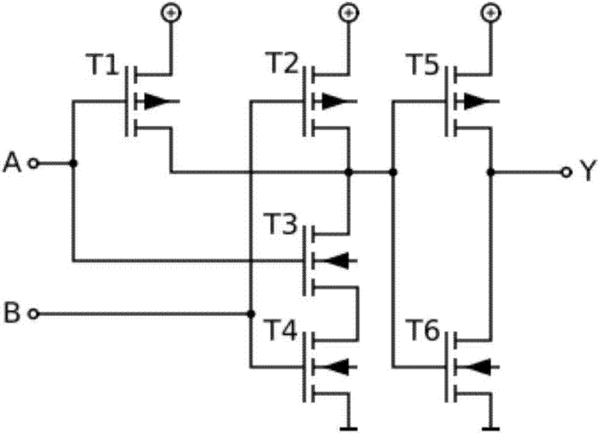
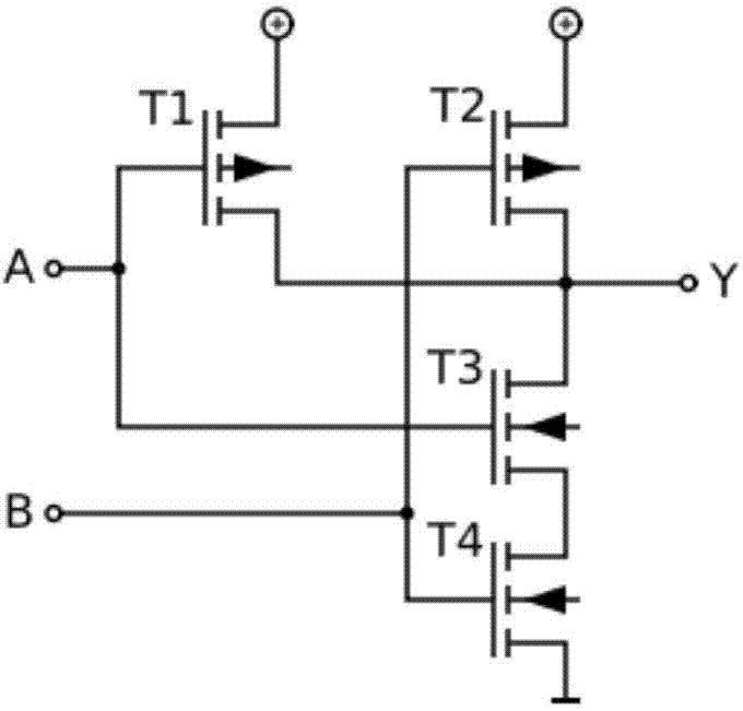
Structure of AND and NOR-logic devices and making method
A logic device and device technology, applied in the field of integrated circuit manufacturing, can solve the problems of large chip area, high cost, complex circuit structure, etc., and achieve the effect of reducing manufacturing cost, simple timing control, and simple device and circuit structure
- Summary
- Abstract
- Description
- Claims
- Application Information
AI Technical Summary
Problems solved by technology
Method used
Image

Examples
Embodiment Construction
[0040] In order to have a more specific understanding of the technical content, characteristics and effects of the present invention, now in conjunction with the accompanying drawings, the details are as follows:
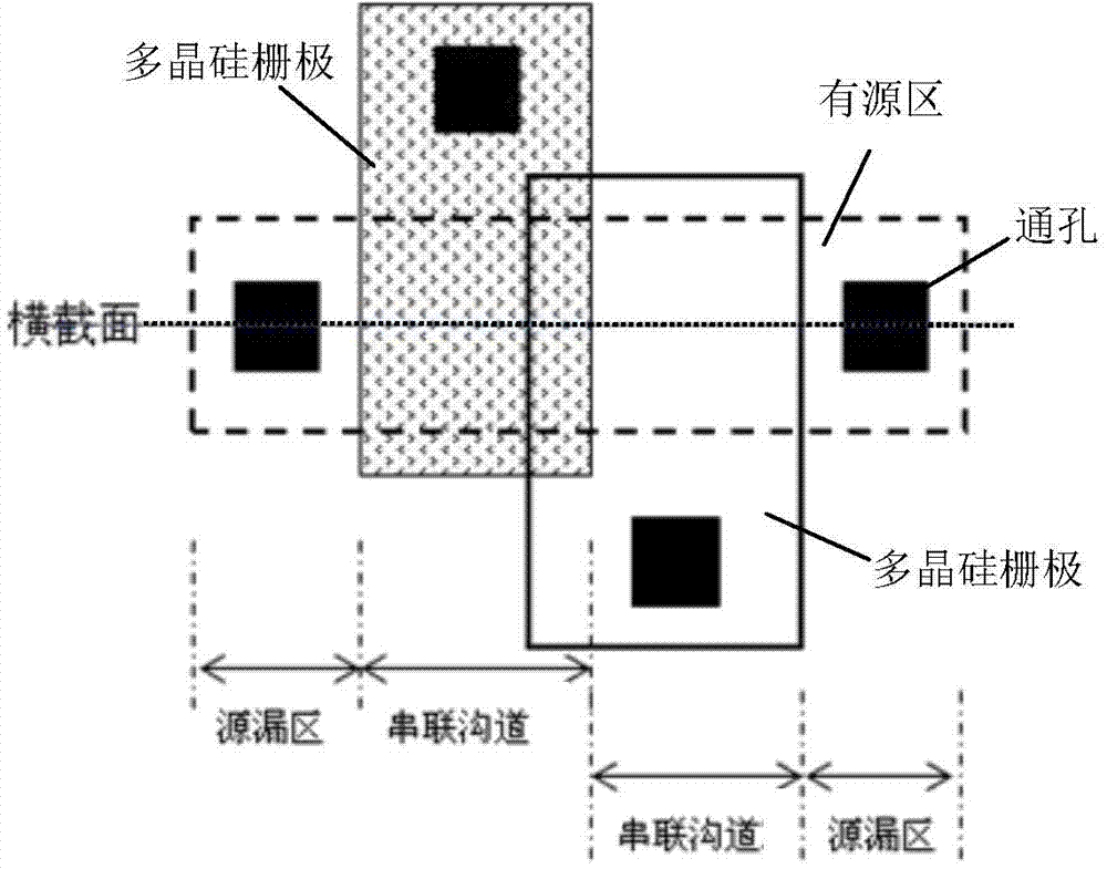
[0041] For the logic device structure of the present invention, please refer to image 3 , 4 shown.
[0042] And logic devices are fabricated in p-well or p-type substrates. There are two adjacent gates on the top, each of which controls the adjacent n-type conductive channel below it. There is a highly doped n-type source region and a drain region at both ends of the gate control gate, and the source region, two channels and the drain region form a series channel with leads at both ends. There is a polysilicon gate above the two gate control gates respectively, and the two polysilicon gates can be separated from each other, adjacent to each other or overlap each other, but they must be electrically isolated from each other and drawn out independently.
[0043] ...
PUM
 Abstract
Description
Claims
Application Information
 - R&D Engineer
- R&D Manager
- IP Professional
- Industry Leading Data Capabilities
- Powerful AI technology
- Patent DNA Extraction
Browse by: Latest US Patents, China's latest patents, Technical Efficacy Thesaurus, Application Domain, Technology Topic, Popular Technical Reports.
© 2024 PatSnap. All rights reserved.Legal|Privacy policy|Modern Slavery Act Transparency Statement|Sitemap|About US| Contact US: help@patsnap.com