A Multilayer Substrate Integrated Waveguide Array Antenna

A substrate-integrated waveguide and array antenna technology, which is applied in antennas, antenna arrays, waveguide horns, etc., can solve the problems that the antenna cannot meet the wide-band working requirements, the feed network is complicated, and the unfavorable high efficiency, etc., so as to facilitate the miniaturization of the system and integrated applications, high efficiency, and the effect of good impedance matching characteristics

Active Publication Date: 2017-12-05
XIDIAN UNIV
View PDF6 Cites 0 Cited by
  • Summary
  • Abstract
  • Description
  • Claims
  • Application Information

AI Technical Summary

Problems solved by technology

[0004] Part of the research on high-gain array antennas based on substrate-integrated waveguide technology focuses on waveguide slot antennas to solve the problems of high processing accuracy and high cost. The working requirements of the petal, and because the feed network is complex, it is not conducive to achieving high efficiency

Method used


Image

  • A Multilayer Substrate Integrated Waveguide Array Antenna
  • A Multilayer Substrate Integrated Waveguide Array Antenna
  • A Multilayer Substrate Integrated Waveguide Array Antenna

Examples


Embodiment Construction

[0040] The present invention will be described in further detail below in conjunction with accompanying drawing:

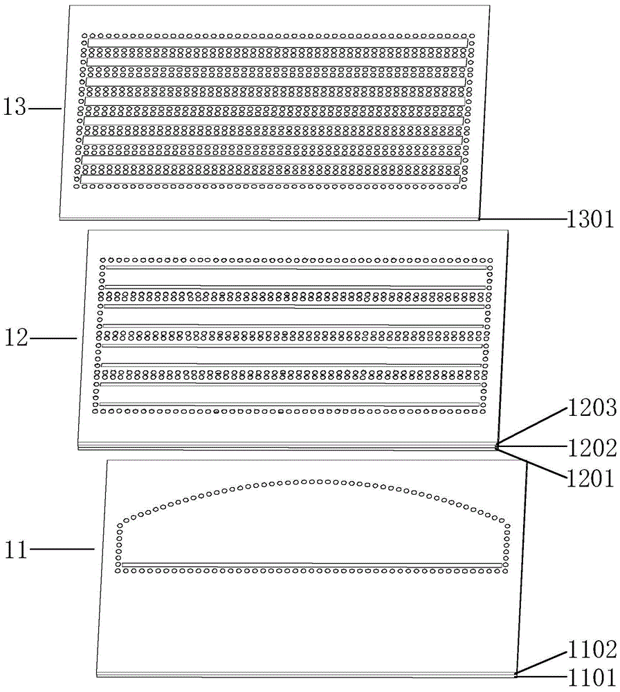
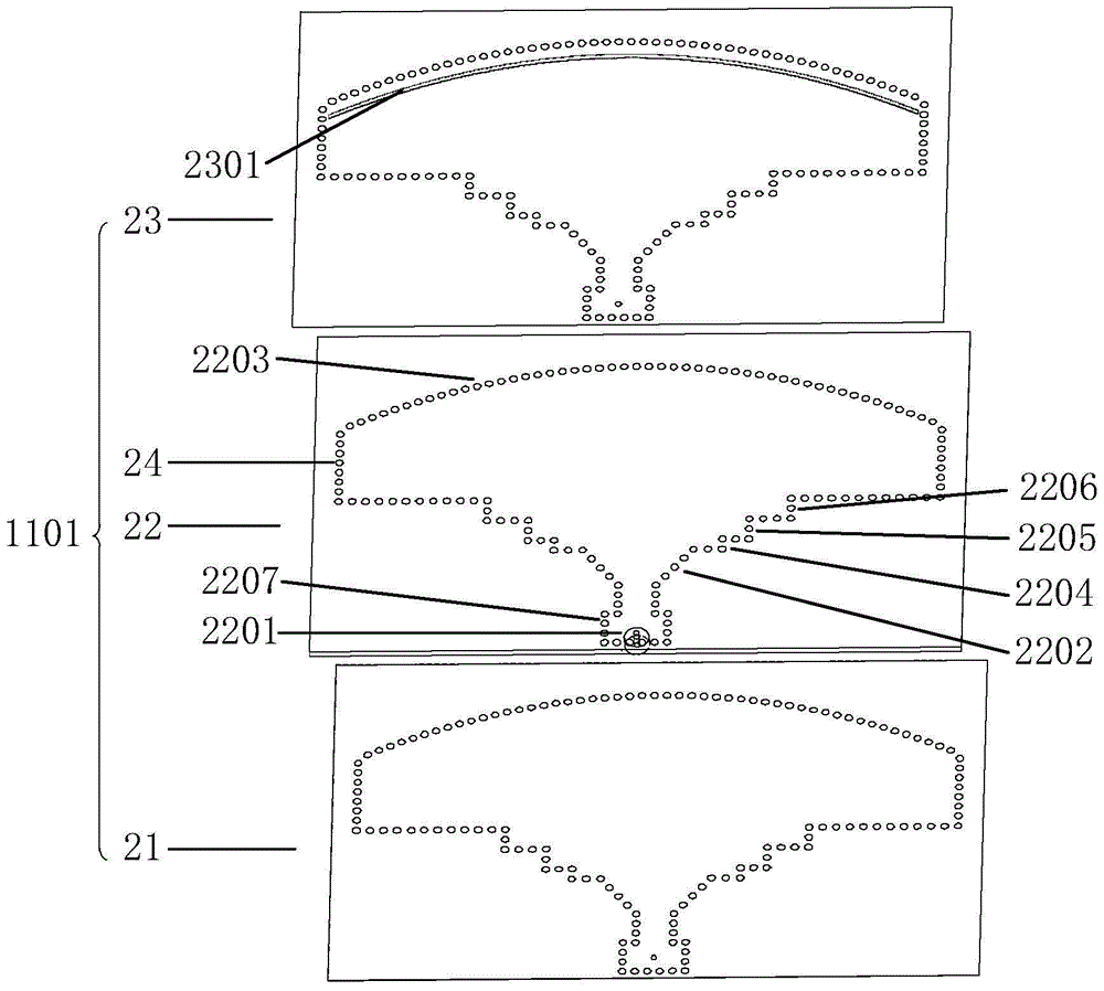
[0041] see Figure 1-Figure 8, a multi-layer substrate integrated waveguide array antenna of the present invention includes a plane wave excitation layer 11, a power divider layer 12 and an antenna radiation layer 13 stacked sequentially from bottom to top; the plane wave excitation layer 11 includes a layer stacked from bottom to top No. 1 lower substrate integrated waveguide 1101 and No. 1 upper substrate integrated waveguide 1102; No. 1 lower substrate integrated waveguide 1101 includes a lower dielectric substrate 22, a lower metallized through hole 24 located on the lower dielectric substrate 22, and a lower dielectric substrate attached to the lower dielectric substrate 22. The lower copper clad layer 21 and the upper copper clad layer 23 on the upper and lower surfaces are provided with a coaxial feed port 2201, a parabolic parabolic substrate integrated wa...


PUM


Abstract

The invention discloses a multi-layer substrate integrated waveguide array antenna, comprising a plane wave excitation layer, a power divider layer and an antenna radiation layer stacked in sequence from bottom to top. The plane wave excitation layer generates a plane wave and is coupled to the power divider Then, the power is distributed reasonably through the power divider layer and fed to the antenna radiation layer. Each antenna element in the antenna radiation layer obtains a reasonable electromagnetic wave amplitude and phase and radiates the electromagnetic wave to the free space. In the present invention, the plane wave excitation layer adopts a plane parabolic plane wave excitation structure, so that the spherical wave is converted into a plane wave with better characteristics in a wider frequency band, so that the antenna of the present invention can meet the working requirements of wide frequency band and low side lobes And achieve high efficiency; by adopting a multilayer substrate integrated waveguide structure in the plane wave excitation layer, the power divider layer and the antenna radiation layer, the overall structure of the antenna of the present invention is simple and compact, easy to process, low in cost, and convenient for system miniaturization and integrated application. .

Description

technical field [0001] The invention belongs to the technical field of antennas, in particular to a multi-layer substrate integrated waveguide array antenna. Background technique [0002] Traditional parabolic antennas can convert spherical waves into plane waves within a broadband range, but due to their large size, complex processing, and difficulty in portability, they do not meet the needs of modern communication systems for miniaturization and integration. The waveguide slot antenna array has excellent characteristics such as low profile, good mechanical strength, compact structure, high aperture efficiency, and low loss. its application. [0003] The substrate-integrated waveguide adopts the Printed Circuit Board (PCB) process or the Low Temperature Co-fired Ceramic (LTCC) process to form two rows of closely arranged parallel metallized through holes on the dielectric substrate. , due to the small spacing of the through holes, the electromagnetic wave can be limited ...

Claims


Application Information

Patent Timeline
Patent Type & Authority Patents(China)
IPC IPC(8): H01Q1/50H01Q13/02H01Q1/38H01Q21/00
Inventor 张天龄杨晓强陈蕾
Owner XIDIAN UNIV
Why Eureka
Try Eureka