Adhesive film, dicing/die-bonding film, method for manufacturing semiconductor device, and semiconductor device
A technology of die-bonding film and manufacturing method, which is applied in the direction of film/sheet adhesive, semiconductor/solid-state device manufacturing, semiconductor device, etc., can solve the coating amount of paste adhesive, coating shape deviation, Difficulty in homogenization and the need for special equipment, etc., to prevent the communication speed from decreasing and improve the yield
- Summary
- Abstract
- Description
- Claims
- Application Information
AI Technical Summary
Problems solved by technology
Method used
Image

Examples
no. 1 Embodiment approach
[0103] A first embodiment of the present invention is an adhesive film for embedding a first semiconductor element fixed on an adherend and for fixing a second semiconductor element different from the first semiconductor element to the adherend. things,
[0104] It is at 120°C and the shear rate is 50s -1 The melt viscosity under is 50 Pa·s or more and 500 Pa·s or less.
Embodiment approach 1-1
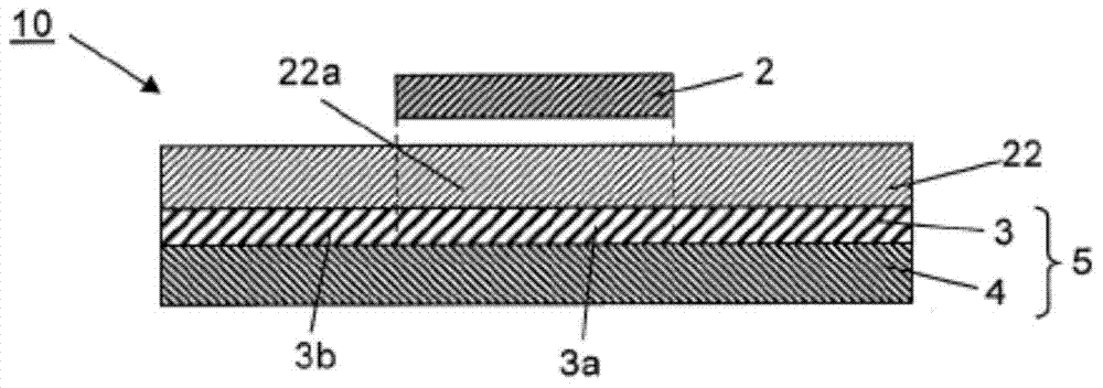
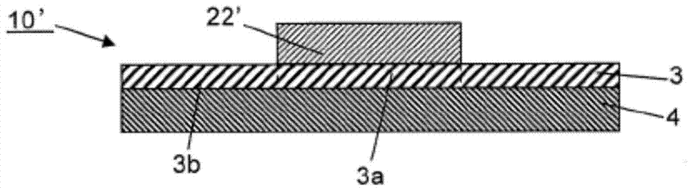
[0106] In Embodiment 1-1, such as figure 1 As shown, the following description will be made taking, as an example, the form of a dicing / die-bonding film in which an adhesive film 22 for embedding is laminated on a dicing film 5 in which an adhesive layer is laminated on a substrate 4 3 made. In this embodiment mode, a mode in which the electrical connection between the adherend and the first semiconductor element is realized by wire bonding connection will be described.
[0107] Adhesive film
[0108] In the adhesive film 22, at 120°C and at a shear rate of 50s -1 The melt viscosity under is set to 50 Pa·s or more and 500 Pa·s or less. The lower limit of the melt viscosity is preferably 60 Pa·s or more, more preferably 70 Pa·s or more. The upper limit of the melt viscosity is preferably 400 Pa·s or less, more preferably 300 Pa·s or less. By adopting the above-mentioned upper limit, when using the adhesive film to fix the second semiconductor element to the adherend, th...
Embodiment approach 1-2
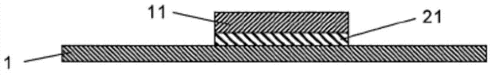
[0235] In Embodiment 1-1, the step of fixing the first semiconductor element to the adherend is performed by bonding a film, and the electrical connection between the two is realized by wire bonding, while in Embodiment 1-2, by using The flip-chip connection of the protruding electrodes of the first semiconductor element realizes the fixing and electrical connection between the two. Therefore, Embodiment 1-2 differs from Embodiment 1-1 only in the fixing method in the first fixing step, and therefore the difference will be mainly described below.
[0236] 1st fixed process
[0237] In this embodiment, in the aforementioned first fixing step, the first semiconductor element 41 is fixed to the adherend 1 by flip-chip connection (see Figure 4A ). In the flip-chip connection, the circuit surface of the first semiconductor element 41 faces the adherend 1, so-called face-down mounting. A plurality of protruding electrodes 43 such as bumps are provided on the first semiconducto...
PUM
| Property | Measurement | Unit |
|---|---|---|
| storage modulus | aaaaa | aaaaa |
| particle size | aaaaa | aaaaa |
| thickness | aaaaa | aaaaa |
Abstract
Description
Claims
Application Information
 - R&D
- Intellectual Property
- Life Sciences
- Materials
- Tech Scout
- Unparalleled Data Quality
- Higher Quality Content
- 60% Fewer Hallucinations
Browse by: Latest US Patents, China's latest patents, Technical Efficacy Thesaurus, Application Domain, Technology Topic, Popular Technical Reports.
© 2025 PatSnap. All rights reserved.Legal|Privacy policy|Modern Slavery Act Transparency Statement|Sitemap|About US| Contact US: help@patsnap.com