Array substrate, display panel and display device

An array substrate and insulating layer technology, applied in the field of liquid crystal display devices, can solve the problems of large load of TFT array substrate, reduced touch sensitivity of touch panel, long charging time of touch electrodes, etc., so as to reduce parasitic capacitance and shorten charging time, the effect of improving touch sensitivity

Active Publication Date: 2015-06-24
BEIHAI HKC OPTOELECTRONICS TECH CO LTD
View PDF3 Cites 17 Cited by
  • Summary
  • Abstract
  • Description
  • Claims
  • Application Information

AI Technical Summary

Problems solved by technology

[0004] In the TFT array substrate of the existing In Cell touch screen, the parasitic capacitance between the signal transmission line and the common electrode is relatively large, which leads to an excessive load on the TFT array substrate, which makes the charging time of the touch electrode longer and reduces the The touch sensitivity of the touch panel

Method used


Image

  • Array substrate, display panel and display device
  • Array substrate, display panel and display device
  • Array substrate, display panel and display device

Examples


Embodiment Construction

[0016] In order to make the objectives, technical solutions, and beneficial effects of the present invention clearer and more complete, the specific embodiments of the present invention will be described in detail below with reference to the accompanying drawings.

[0017] The embodiment of the present invention provides an array substrate. See the following examples for details.

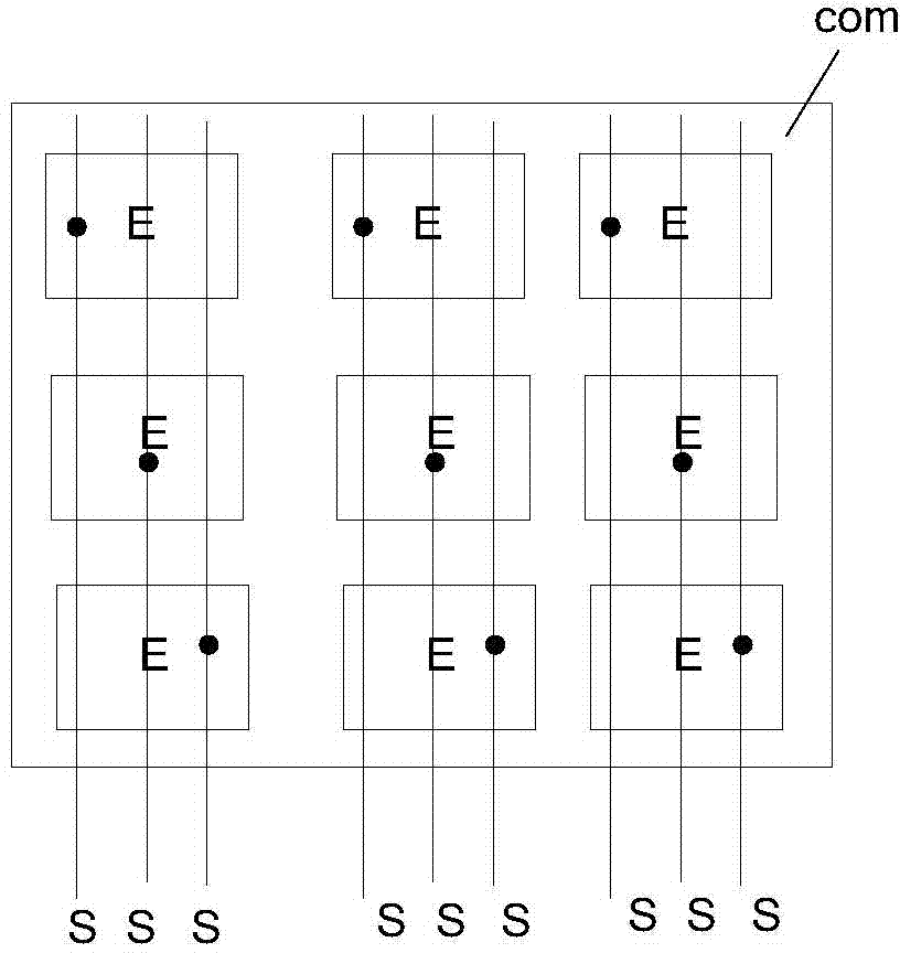
[0018] The array substrate provided by the embodiment of the present invention may have a structure in which the common electrode layer is below the pixel electrode layer, that is, the Middle-Com structure. The schematic diagram of the array substrate of the Middle-Com structure is as figure 2 Shown.

[0019] First introduce the structure of the array substrate of the Middle-Com structure, please refer to figure 2 .

[0020] Such as figure 2 As shown, the structure of the array substrate is as follows, which includes:

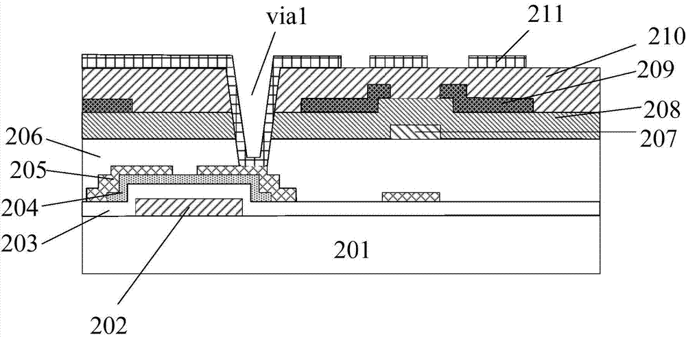
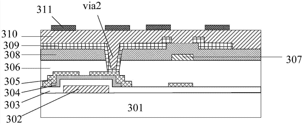
[0021] Substrate 201;

[0022] The gate layer 202 on the substrate 201;

[0023] A gate ...


PUM


Abstract

The invention provides an array substrate. The array substrate comprises a substrate body, wherein a signal transmission line, a first insulating layer, a second insulating layer, a pixel electrode layer and a public electrode layer are located on the substrate body, the first insulating layer is located between the signal transmission line and the public electrode layer, the second insulating layer is located between the pixel electrode layer and the public electrode layer, the dielectric constant of the first insulating layer is smaller than or equal to that of the second insulating layer, and the signal transmission line is electrically connected with the public electrode layer. By means of the array substrate, the parasitic capacitance between the signal transmission line and the public electrode layer or the pixel electrode layer is reduced. Due to the reduction of the parasitic capacitance, the reduction of loads on a touch control panel is facilitated, the charging time of a touch control electrode is shortened as well, and the touch control sensitivity of the touch control panel is improved. The invention further provides a display panel and a display device.

Description

Technical field [0001] The present invention relates to the field of liquid crystal display devices, in particular to an array substrate, a display panel and a display device. Background technique [0002] Compared with the touch display device in which the touch panel is arranged on the liquid crystal display panel, the touch display device integrating the touch display device and the liquid crystal display panel can reduce the use of substrates and has the advantage of thinner thickness, which has become the mainstream touch display today. Device. The touch display device integrated with the touch display device and the liquid crystal display panel includes an on-cell structure and an in-cell structure. Among them, the in-cell structure refers to embedding the touch panel function into the TFT array substrate. [0003] Currently, the touch electrodes of the self-capacitive in cell touch screen are multiplexed with the common electrodes. Such as figure 1 As shown, the common el...

Claims


Application Information

Patent Timeline
Patent Type & Authority Applications(China)
IPC IPC(8): G02F1/1343G02F1/1362H01L27/12G06F3/041
CPCG02F1/133345G02F1/13338G02F1/134363G02F1/136227G02F1/136286G06F3/0412H01L27/1214H01L27/1248H01L27/124G02F1/134372
Inventor 袁永于泉鹏崔萌黄忠守
Owner BEIHAI HKC OPTOELECTRONICS TECH CO LTD
Why Eureka
Try Eureka