PCB of LED indicator board for automobile instrument and design method of PCB
A technology for PCB boards and automotive instruments, which is applied to printed circuit parts, electrical components, circuits, etc., can solve the problems of easy damage of LEDs, unfavorable LED heat export, etc., and achieve the effects of avoiding damage, high thermal conductivity, and prolonging service life
- Summary
- Abstract
- Description
- Claims
- Application Information
AI Technical Summary
Problems solved by technology
Method used
Image
Examples
specific Embodiment approach 1
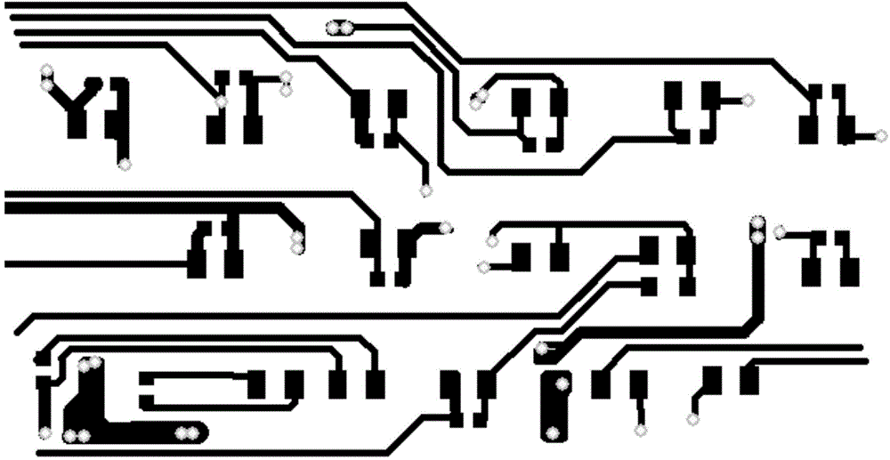
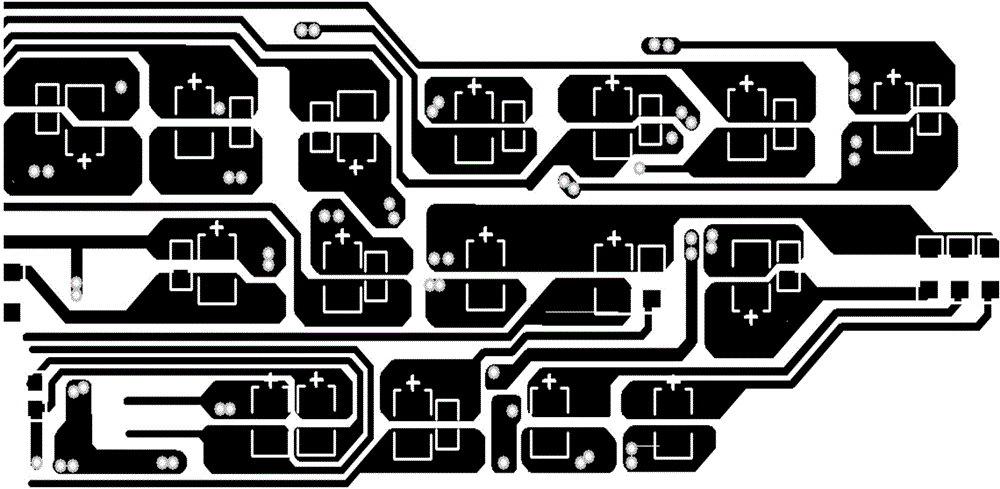
[0016] Specific implementation mode one: refer to figure 2 Specifically explain this embodiment, the PCB board of the LED indicator board for automobile instrument described in this embodiment, the two pads of each LED are covered with a large-area copper clad layer, and the area of the copper clad layer is larger than that of the LED solder. 3 times the disk area.
[0017] In the PCB board of the LED indicator board for automobile instrument described in this embodiment, the two welding pads of each LED are covered with a large-area copper clad layer. Since copper has good thermal conductivity, this structure is very beneficial. The heat generated by the two electrodes of the LED leads to the copper clad layer and then dissipates, which effectively prevents the LED from being damaged due to the long working time and temperature rise, and prolongs the service life of the LED.
specific Embodiment approach 2
[0018] Specific embodiment 2: This embodiment is a further description of the PCB board of the LED indicator board for automotive instrumentation described in the specific embodiment 1. In this embodiment, the areas of the copper clad layers at the two pads of the same LED are equal .
[0019] Due to the large negative bracket of the LED bracket, the temperature generated by the negative pole during the LED lighting process will be relatively high. Therefore, increasing the copper clad area at the pad corresponding to the LED negative pin can meet the requirements of the manufacturing process characteristics of the LED itself. The purpose of increasing the copper clad area on the pad corresponding to the LED positive pin on the PCB is to meet the characteristics of the welding process, because if the copper clad area of the two pads of the LED differs greatly, it will cause two solder pads in the soldering process. The heating rate of each pad is inconsistent, which increase...
specific Embodiment approach 3
[0020] Specific embodiment three: this embodiment is to further illustrate the PCB board of the LED indicator board for automobile instrument described in specific embodiment one or two. short sides parallel to each other.
[0021] The PCB boards of the LED indicator boards for automobiles are all rectangular, and the length is much greater than the width. In this embodiment, the LEDs are arranged along the length direction of the short side of the printed board. In the process of practical application, due to factors such as the temperature rise of the printed board, it will cause deformation, that is, the rectangular bottom plate is bent and deformed, and the deformation method is that the long side is bent. If the original design method is used, the LEDs are parallel to the long side. This leads to longer or shorter distance between the two pads of the LED under the premise of deformation of the PCB, which in turn causes stress between the two pins of the LED to be welded, ...
PUM
 Abstract
Description
Claims
Application Information
 - R&D Engineer
- R&D Manager
- IP Professional
- Industry Leading Data Capabilities
- Powerful AI technology
- Patent DNA Extraction
Browse by: Latest US Patents, China's latest patents, Technical Efficacy Thesaurus, Application Domain, Technology Topic, Popular Technical Reports.
© 2024 PatSnap. All rights reserved.Legal|Privacy policy|Modern Slavery Act Transparency Statement|Sitemap|About US| Contact US: help@patsnap.com


