Semiconductor device and forming method thereof

A technology of semiconductors and devices, which is applied in the field of semiconductor devices and their formation, can solve the problems that are not enough to improve the operating speed of semiconductor devices, the degree of carrier mobility is limited, and the drain induction barrier is reduced, so as to improve the electrical performance, increased carrier mobility, and improved threshold voltage

Active Publication Date: 2015-06-10
SEMICON MFG INT (SHANGHAI) CORP
View PDF4 Cites 2 Cited by
  • Summary
  • Abstract
  • Description
  • Claims
  • Application Information

AI Technical Summary

Problems solved by technology

[0005] However, in practical applications, it has been found that the degree of improvement in carrier mobility of semiconductor devices formed by existing technologies is limited, which is not enough to meet the needs of increasing the operating speed of semiconductor devices, and there are problems such as lowering of the drain induction barrier and leakage current.

Method used


Image

  • Semiconductor device and forming method thereof
  • Semiconductor device and forming method thereof
  • Semiconductor device and forming method thereof

Examples


Embodiment Construction

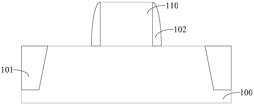
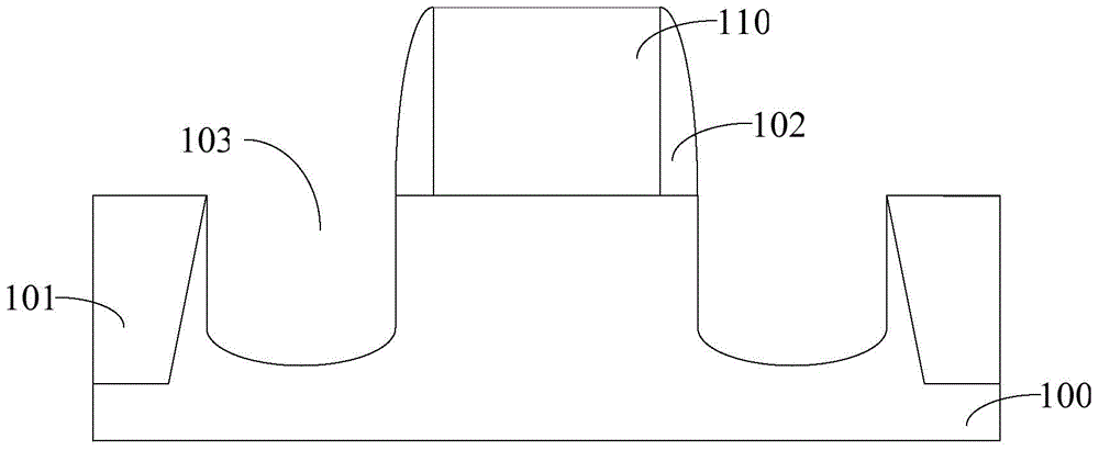
[0036] It can be seen from the background art that the carrier mobility of the semiconductor device formed in the prior art is limited, and there are problems such as the decrease of the drain induction barrier and the leakage current.

[0037] In order to solve the above-mentioned problems, research is conducted on the formation process of semiconductor devices. The formation process of semiconductor devices includes the following steps, please refer to figure 1 : Step S1, providing a semiconductor substrate, and a gate structure is formed on the surface of the semiconductor substrate; Step S2, performing first ion implantation on the semiconductor substrate on both sides of the gate structure to form a lightly doped region (LDD) ; Step S3, performing second ion implantation on the semiconductor substrate close to the channel region on both sides of the lightly doped region to form a pocket region (Pocket); Step S4, forming sidewalls on both sides of the gate structure; step ...


PUM


Abstract

A semiconductor device and a forming method thereof are provided. The forming method of the semiconductor device comprises the following steps: providing a semiconductor substrate and a dummy gate structure; etching the semiconductor substrate at the two sides of the dummy gate structure to form first grooves; forming first stress layers filling the first grooves; performing etching to remove the dummy gate structure and part of the semiconductor substrate in the thickness direction, and forming a second groove in the semiconductor substrate; forming a second stress layer filling the second groove, wherein the stress type of the second stress layer and the stress type of the first stress layers are opposite, and the top of the second stress layer is lower than the surface of the semiconductor substrate; forming an intrinsic material layer filling the second groove, wherein the intrinsic material layer is disposed on the surface of the second stress layer; and forming a gate structure on the surface of the intrinsic material layer, wherein the gate structure includes a gate dielectric layer and a gate conductive layer. The carrier mobility of the channel region of the semiconductor device is improved, the operating speed of the semiconductor device is optimized, and the electrical performance of the semiconductor device is improved.

Description

technical field [0001] The invention relates to the technology in the field of semiconductor manufacturing, in particular to a semiconductor device and a forming method thereof. Background technique [0002] With the continuous development of semiconductor technology, carrier mobility enhancement technology has been widely studied and applied. Improving the carrier mobility in the channel region can increase the driving current of semiconductor devices and improve the performance of devices. [0003] In the existing manufacturing process of semiconductor devices, since stress can change the energy gap and carrier mobility of silicon materials, it has become more and more common means to improve the performance of semiconductor devices through stress. Specifically, by properly controlling the stress, the mobility of carriers (electrons in NMOS devices, holes in PMOS devices) can be increased, thereby increasing the driving current, thereby greatly improving the performance of...

Claims


Application Information

Patent Timeline
Patent Type & Authority Applications(China)
IPC IPC(8): H01L21/336H01L21/762H01L29/78H01L29/10
CPCH01L29/66545H01L29/1054H01L29/165H01L29/66636H01L29/66651
Inventor 赵猛
Owner SEMICON MFG INT (SHANGHAI) CORP
Why Eureka
Try Eureka