A method of manufacturing a semiconductor planarization layer
A planarization layer and manufacturing method technology, which is applied in semiconductor/solid-state device manufacturing, photoplate process of patterned surface, optics, etc., can solve insufficient solvent precipitation, large thickness of planarization layer, surface hardening of planarization layer, etc. problem, to achieve the effect of improving reliability, optimizing taper angle and ensuring consistency
- Summary
- Abstract
- Description
- Claims
- Application Information
AI Technical Summary
Problems solved by technology
Method used
Image

Examples
Embodiment 1
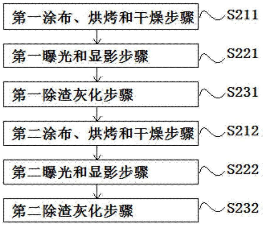
[0037] figure 1 It is a flow chart showing the process of completing the planarization layer by applying glue twice in Embodiment 1 of the present invention. In the manufacturing method of the semiconductor planarization layer described in this embodiment, the glue coating operation of the planarization layer is implemented twice, and the thickness of each glue coating is set to 1.5 μm. The manufacturing method includes the following steps implemented in sequence:
[0038] The first coating, baking and drying step S211: coating the photoresist used to form the first planarization layer on the lower layer film with a thickness of 1.5 μm, and softening the first planarization layer after coating Baking treatment, and further using a vacuum drying device to implement low-temperature drying treatment to remove the solvent in the first planarization layer;
[0039] The first exposure and development step S221: performing exposure treatment and development treatment on the first p...
Embodiment 2
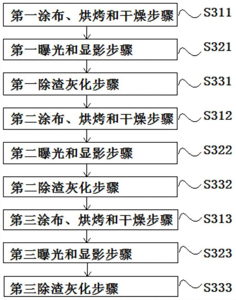
[0047] figure 2 It is a flow chart showing the three times of gluing to complete the planarization layer in Embodiment 2 of the present invention. In the manufacturing method of the semiconductor planarization layer in this embodiment, the glue coating operation of the planarization layer is implemented three times, and the thickness of each glue coating is set to 1 μm. The manufacturing method includes the following steps implemented in sequence:
[0048] The first coating, baking and drying step S311: Coating the photoresist for forming the first planarization layer on the lower layer film with a thickness of 1 μm, and performing soft baking on the first planarization layer after coating treatment, and further use a vacuum drying device to implement low-temperature drying treatment to remove the solvent in the first planarization layer;
[0049] First exposure and development step S321: performing exposure treatment and development treatment on the first planarization laye...
Embodiment 3
[0059] Except not carrying out all deslagging and ashing steps, it carried out similarly to Example 1, and obtained the final planarization layer. As a result, the solvent precipitation rate of the photoresist in the finally formed planarization layer can reach about 93%, the total film thickness uniformity of the finally formed planarization layer can reach about 8-15%, and the taper of the planarization layer The angle can reach about 40-60°.
PUM
| Property | Measurement | Unit |
|---|---|---|
| thickness | aaaaa | aaaaa |
| thickness | aaaaa | aaaaa |
| thickness | aaaaa | aaaaa |
Abstract
Description
Claims
Application Information
 - R&D
- Intellectual Property
- Life Sciences
- Materials
- Tech Scout
- Unparalleled Data Quality
- Higher Quality Content
- 60% Fewer Hallucinations
Browse by: Latest US Patents, China's latest patents, Technical Efficacy Thesaurus, Application Domain, Technology Topic, Popular Technical Reports.
© 2025 PatSnap. All rights reserved.Legal|Privacy policy|Modern Slavery Act Transparency Statement|Sitemap|About US| Contact US: help@patsnap.com