
Low Noise Low Voltage Differential Signal Transmitter

A low-voltage differential signal, differential signal technology, applied in differential amplifiers, improved amplifiers to reduce noise effects, DC-coupled DC amplifiers, etc., can solve problems such as affecting common-mode levels, improve matching, and reduce common-mode noise. , the effect of reducing the impact

Active Publication Date: 2017-05-10
BRITE SEMICON SHANGHAI CORP
View PDF5 Cites 0 Cited by
  • Summary
  • Abstract
  • Description
  • Claims
  • Application Information

AI Technical Summary

Problems solved by technology

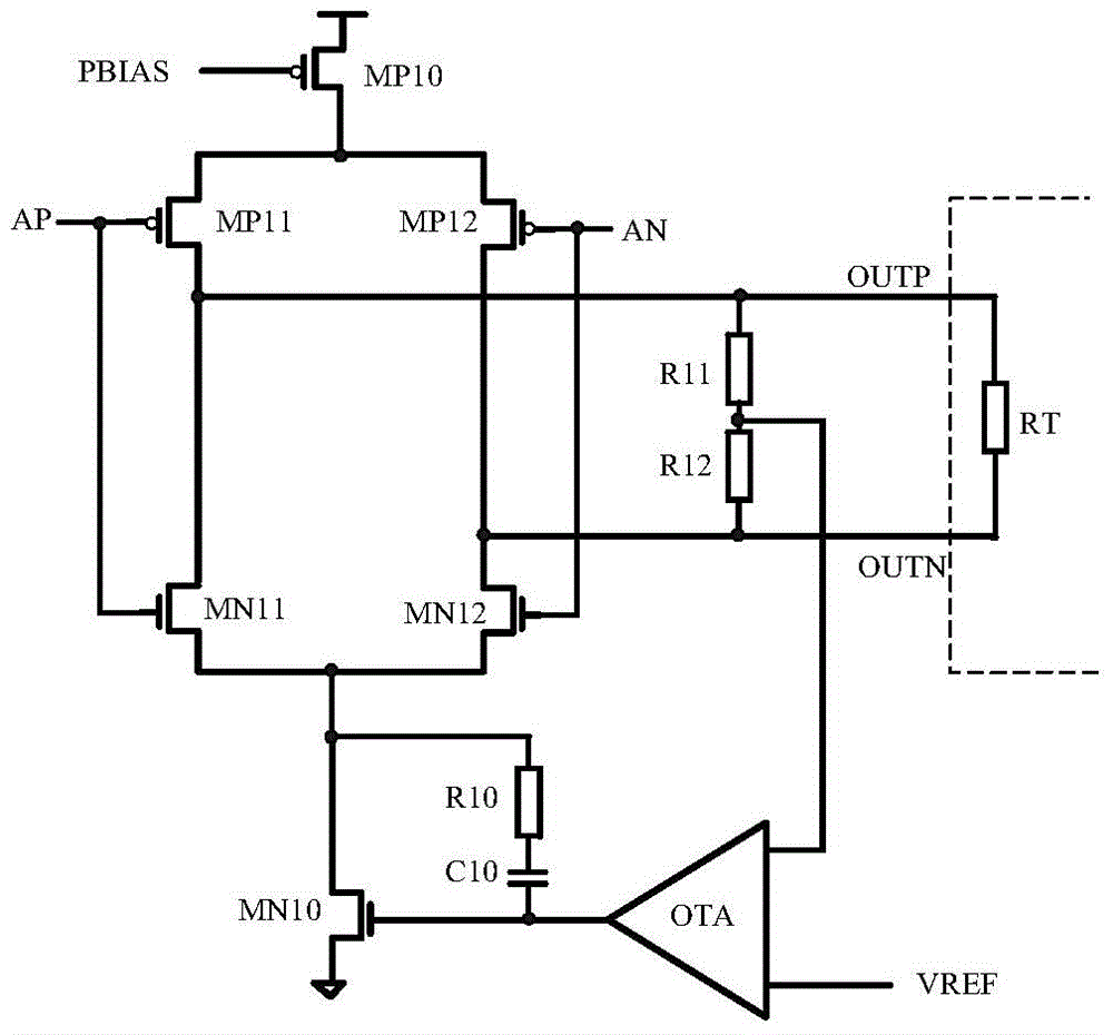
In the low-voltage differential signal transmission circuit in the prior art, the charge injection during the switching process of MP11, MP12, MN11, and MN12, and the effects of the compensation resistor R10 and the compensation capacitor C10 on the output coupling will affect the common-mode level and introduce common-mode noise

Method used


Image

  • Low Noise Low Voltage Differential Signal Transmitter
  • Low Noise Low Voltage Differential Signal Transmitter
  • Low Noise Low Voltage Differential Signal Transmitter

Examples


Embodiment Construction

[0023] In order to make the above objectives, features and advantages of the present invention more obvious and understandable, the present invention will be further described in detail below with reference to the accompanying drawings and specific embodiments.

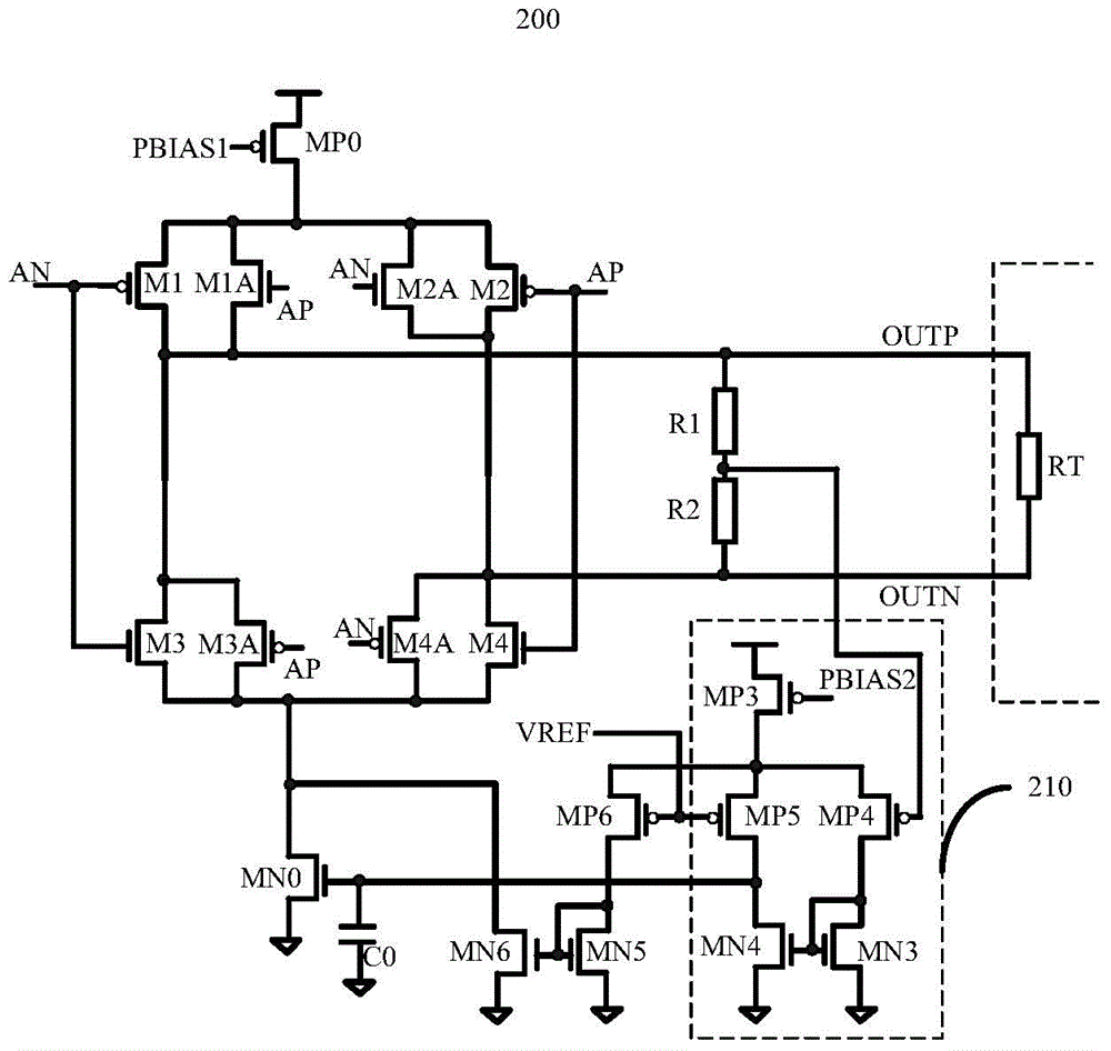
[0024] figure 2 It is a schematic circuit diagram of the low-voltage differential signal transmitter 100 in an embodiment of the present invention. Such as figure 2 As shown, the low-voltage differential signal transmitter 100 includes a transistor MP0, a transistor M1, a transistor M2, a transistor M3, a transistor M4, a transistor MN0, voltage dividing resistors R1 and R2, a transconductance amplifier 210, transistors MP6, MN5 and MN6, Compensation capacitor C0, transistors M1A, M2A, M3A and M4A. The transconductance amplifier 210 includes a transistor MP3. The transistors MP0, M1, M2, M3A, M4A, MP6, and MP3 are PMOS transistors, and the transistors MN0, M3, M4, M1A, M2A, MN6, and MN5 are NMOS transistors.

[0025] T...


PUM


Abstract

The invention provides a low-voltage differential signal transmitter. The low-voltage differential signal transmitter comprises transistors MP0, M1, M2, M3, M4, MN0, divider resistors R1 and R2, a transconductance amplifier, transistors MP6, MN5 and MN6 and a compensation capacitor C0, wherein the divider resistors R1 and R2 and a load resistor RT are connected at a first output end OUTP and a second output end OUTN in series, the transconductance amplifier comprises a transistor MP3, the first input end of the transconductance amplifier is connected with intermediate nodes of the divider resistors R1 and R2, the second input end of the transconductance amplifier is connected with VREF, and the output end of the transconductance amplifier is connected with a gate of the transistor MN0. The divider resistors R1 and R2, the compensation capacitor C0, the transconductance amplifier and the transistors MP6, MN5, MN6 and MN0 form a common-mode feedback circuit. Because zero points are added to the transistors MP6, MN5, MN6 and MN0 and loop compensation is achieved, a coupled access where a compensation resistor R0 and the compensation capacitor C0 are located in the prior art is avoided, and common-mode noise is lowered.

Description

[0001] 【Technical Field】 [0002] The invention relates to the field of circuit design, in particular to a low-noise low-voltage differential signal transmitter. [0003] 【Background technique】 [0004] With the development of semiconductor and computer technology, the clock frequency on integrated circuit chips has reached GHz. The demand for high-speed data transmission rates between chips is far greater than Gb / s. LVDS (Low Voltage Differential Signaling) is a low-swing differential signal technology, which has the characteristics of high data transmission speed, low noise and low power consumption, and is widely used in the field of high-speed digital interfaces. [0005] In actual design, there are many undesirable factors (such as incompletely matched terminal resistance, transmission line effects, noise) that affect the performance of the driver. The traditional low-voltage differential signal transmitter is affected by the non-ideality of the switch and the common mode feedba...

Claims


Application Information

Patent Timeline
Patent Type & Authority Patents(China)
IPC IPC(8): H03F3/45H03F1/26
Inventor 王汉祥周玉镇戴颉李耿民职春星
Owner BRITE SEMICON SHANGHAI CORP
Learn More