Preparation method of nanoporous structures on surfaces of silicon wafers
A technology of nanoporous structure and silicon wafer surface, applied in the process of producing decorative surface effects, microstructure technology, microstructure devices, etc.
- Summary
- Abstract
- Description
- Claims
- Application Information
AI Technical Summary
Problems solved by technology
Method used
Image

Examples
preparation example Construction
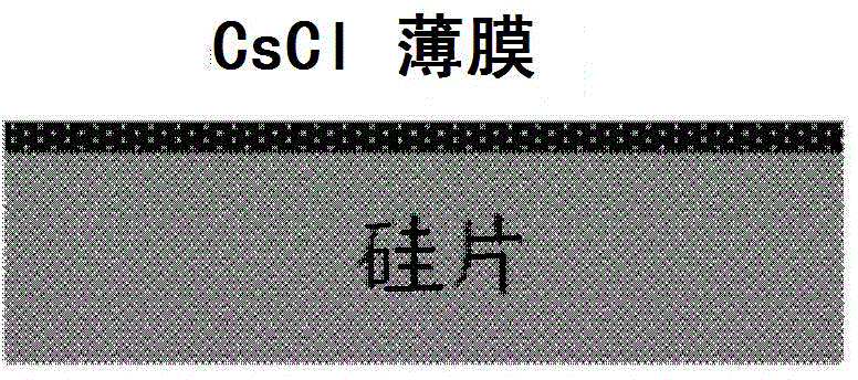
[0029] based on figure 1 The flow chart of the method for preparing the nanopore structure on the surface of a silicon wafer as shown, Figure 2 to Figure 7 It is a process flow chart for preparing a nanopore structure on the surface of a silicon wafer according to an embodiment of the present invention. In this embodiment, the cesium chloride nano-island self-assembly technology and micromachining stripping and plasma deep etching technology are used to complete the silicon surface nanopore structure. The preparation of pore structure, this method comprises the following steps:
[0030] Such as figure 2 As shown, clean the silicon wafer and put it into the vacuum coating chamber to evaporate the cesium chloride thin film with a film thickness of 200-7000 angstroms. The silicon wafer is selected from the silicon wafer used in the semiconductor industry, with a thickness of 0.2mm-0.5mm, P-type, a resistivity of 1Ω·cm-10Ω·cm, and a polished or rough surface.
[0031] Such as...
Embodiment
[0038] The following is a process flow diagram for preparing a nanopore structure on the surface of a silicon wafer according to an embodiment of the present invention. The method includes the following steps:
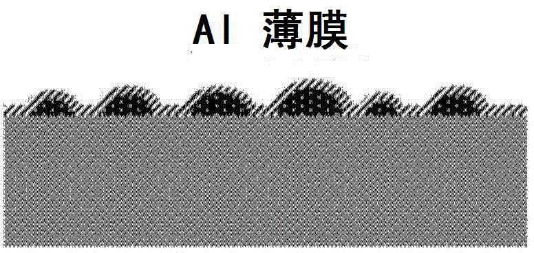
[0039] Step 1: Evaporate a cesium chloride film on a silicon wafer by thermal evaporation, the film thickness is 300 nanometers, and the thickness is measured and controlled by a quartz crystal thickness gauge.
[0040] Step 2: Put the silicon wafer coated with a cesium chloride film into a ventilated chamber with a humidity of 50%, the humidity is controlled by the flow of humid gas flowing into the chamber, develop for 1 hour under this humidity condition, and make the cesium chloride The thin film aggregates into a nano-island structure, and a cesium chloride nano-island structure is formed on the surface of the silicon wafer. The cesium chloride nano-islands have an average diameter of 600 nm.
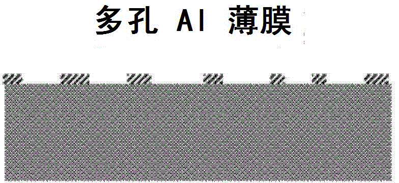
[0041] Step 3: Put the silicon wafer with cesium chloride nano-island...
PUM
| Property | Measurement | Unit |
|---|---|---|
| thickness | aaaaa | aaaaa |
| electrical resistivity | aaaaa | aaaaa |
| diameter | aaaaa | aaaaa |
Abstract
Description
Claims
Application Information
 - Generate Ideas
- Intellectual Property
- Life Sciences
- Materials
- Tech Scout
- Unparalleled Data Quality
- Higher Quality Content
- 60% Fewer Hallucinations
Browse by: Latest US Patents, China's latest patents, Technical Efficacy Thesaurus, Application Domain, Technology Topic, Popular Technical Reports.
© 2025 PatSnap. All rights reserved.Legal|Privacy policy|Modern Slavery Act Transparency Statement|Sitemap|About US| Contact US: help@patsnap.com