
A kind of preparation method of au modified zn/zno micro-nano material

A micro-nano, thermoelectric refrigerator technology, applied in nanotechnology, nanotechnology, material excitation analysis, etc., can solve the problems of low economic efficiency, inconvenient operation, difficult control, etc., and achieve high surface-enhanced Raman activity and simple operation. Effect

Inactive Publication Date: 2016-03-23
JILIN UNIV
View PDF5 Cites 0 Cited by
  • Summary
  • Abstract
  • Description
  • Claims
  • Application Information

AI Technical Summary

Problems solved by technology

At present, the effective methods for synthesizing noble metal-modified semiconductors mainly include photocatalytic deposition, displacement method, sputtering method, and hydrothermal method, but these methods have disadvantages such as inconvenient operation, difficult control, and the need for additional light irradiation or reducing agents. In addition, the traditional The surface-enhanced Raman substrates prepared by the method are all disposable, which not only makes their economic benefits low, but also has great limitations in application occasions. For example, it is necessary to analyze different molecules on the same substrate. On this disposable substrate Therefore, it is of great significance to find a method for preparing reusable surface-enhanced Raman substrates with simple operation and easy control.

Method used


Image

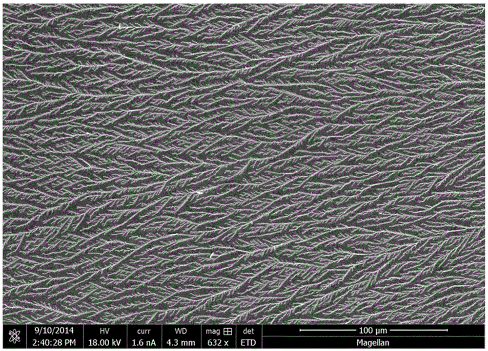
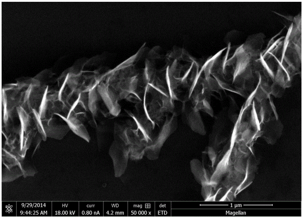
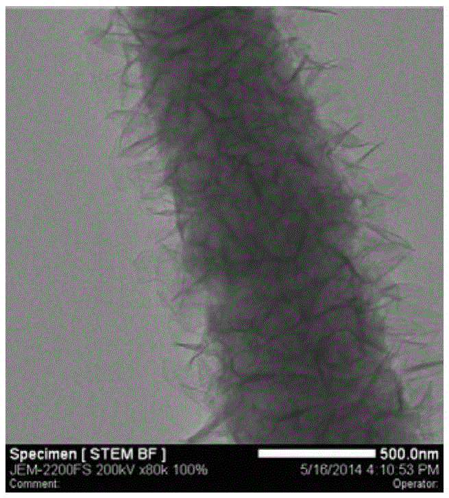
  • A kind of preparation method of au modified zn/zno micro-nano material
  • A kind of preparation method of au modified zn/zno micro-nano material
  • A kind of preparation method of au modified zn/zno micro-nano material

Examples


Embodiment 1

[0030] (1) Use deionized water and configure ZnSO with a concentration of 20mM 4 electrolyte.

[0031] (2) Put the silicon wafer on the TEC in the heat preservation room. The TEC model is TEC1-12705. The heat preservation room is connected to a circulating water bath. On the chip, the interval is 0.8cm. Drop ZnSO between the electrodes 4 Electrolyte, cover with a glass slide.

[0032] (3) Adjust the voltage across the TEC to 3V to freeze the electrolyte quickly, and then adjust the voltage across the TEC to -0.3V to slowly melt the electrolyte. Use an optical microscope to observe the dissolution of the ice layer. When the ice layer is only left For ice nuclei with a diameter of about 0.1 mm, disconnect the voltage at both ends of the TEC, and the ice nuclei will gradually become larger until they fill the space between the two electrodes, and then placed for 30 minutes.

[0033] (4) Apply a DC voltage of 0.8V across the electrodes and deposit for 30 minutes.

[0034] (5)...

Embodiment 2

[0038] (1) Use deionized water and configure ZnSO with a concentration of 50mM 4 electrolyte.

[0039] (2) Put the silicon wafer on the TEC in the heat preservation room. The TEC model is TEC1-12705. The heat preservation room is connected to a circulating water bath. On the chip, the interval is 0.8cm. Drop ZnSO between the electrodes 4 Electrolyte, cover with a glass slide.

[0040](3) Adjust the voltage across the TEC to 3V to freeze the electrolyte quickly, and then adjust the voltage across the TEC to -0.3V to slowly melt the electrolyte. Use an optical microscope to observe the dissolution of the ice layer. When the ice layer is only left For ice nuclei with a diameter of about 0.1 mm, disconnect the voltage at both ends of the TEC, and the ice nuclei will gradually become larger until they fill the space between the two electrodes, and then placed for 30 minutes.

[0041] (4) Apply a DC voltage of 1.4V across the electrodes and deposit for 30 minutes.

[0042] (5) ...

Embodiment 3

[0047] (1) Use deionized water and configure ZnSO with a concentration of 80mM 4 electrolyte.

[0048] (2) Put the silicon wafer on the TEC in the heat preservation room. The TEC model is TEC1-12705. The heat preservation room is connected to a circulating water bath. On the chip, the interval is 0.8cm. Drop ZnSO between the electrodes 4 Electrolyte, cover with a glass slide.

[0049] (3) Adjust the voltage across the TEC to 3V to freeze the electrolyte quickly, and then adjust the voltage across the TEC to -0.3V to slowly melt the electrolyte. Use an optical microscope to observe the dissolution of the ice layer. When the ice layer is only left For ice nuclei with a diameter of about 0.1 mm, disconnect the voltage at both ends of the TEC, and the ice nuclei will gradually become larger until they fill the space between the two electrodes, and then placed for 30 minutes.

[0050] (4) Apply a DC voltage of 1.0V across the electrodes and deposit for 30 minutes.

[0051] (5)...


PUM

PropertyMeasurementUnit
thicknessaaaaaaaaaa
diameteraaaaaaaaaa
diameteraaaaaaaaaa

Abstract

The invention belongs to the technical field of micro-nanometer materials and particularly relates to a method for preparing an Au modified Zn / ZnO micro-nanometer structure function material through the combination of electrochemical deposition and the substitution method. Two electrodes are arranged on a substrate silicon wafer in parallel, ZnSO4 electrolyte is dripped between the electrodes, a glass sheet covers the ZnSO4 electrolyte, the substrate silicon wafer is placed in an insulation room, an ice layer fully spread between the two electrodes is formed between the silicon wafer and the glass sheet by means of a TEC in the insulation room, the substrate silicon wafer is placed in the insulation room for another 30 minutes, then direct-current voltage of 0.8-1.4 V is added between the two electrodes for 30 minutes of deposition, the obtained product is cleaned through deionized water, aired and steeped into a chloroauric acid solution for 30 seconds and then is taken out, cleaned and aired, and therefore an Au modified Zn / ZnO micro-nanometer structure is obtained. According to the method, operation is simple, and the prepared product has high surface-enhanced Raman activity and can be used repeatedly.

Description

technical field [0001] The invention belongs to the technical field of micro-nano functional materials, and in particular relates to a method for preparing Au-modified Zn / ZnO micro-nano-structure functional materials by combining electrochemical deposition and a replacement method. Background technique [0002] Due to the ultra-high sensitivity, fast response and fingerprint effect of the surface-enhanced Raman scattering (SERS) technology, it is widely used in many disciplines, such as chemistry, physics, medicine, biology, life science, etc. For many years, surface-enhanced Raman scattering substrates were mainly limited to pure noble metal (eg gold, silver) nanostructures. Recent studies have shown that different kinds of semiconductors such as ZnO, ZnS, TiO 2 , CuO can also produce weak surface-enhanced Raman activity with an enhancement factor in the range of 10 -1 ~10 -3 between. Therefore, many researchers are devoted to the study of noble metal and semiconductor ...

Claims


Application Information

Patent Timeline
Patent Type & Authority Patents(China)
IPC IPC(8): B22F1/00C25D9/04G01N21/65B82Y30/00B82Y40/00
Inventor 张明喆肖传海
Owner JILIN UNIV
Learn More