Supercharge Your Innovation With Domain-Expert AI Agents!

High-resistance silicon substrate based LDMOS MMIC chip

A high-resistance silicon and chip technology, applied in the field of LDMOS MMIC chips, can solve the problems of reducing LDMOS MMIC performance, reducing inductance Q and self-resonant frequency, increasing parasitic capacitance to ground, etc., to increase bandwidth and power conversion efficiency, and reduce PN junction capacitance, increasing the effect of isolation

Inactive Publication Date: 2015-03-04
江苏博普电子科技有限责任公司
View PDF5 Cites 0 Cited by
  • Summary
  • Abstract
  • Description
  • Claims
  • Application Information

AI Technical Summary

Problems solved by technology

However, the isolation between the low-resistance and heavily doped P-type substrate and the top-layer metal as the ground does not exceed 10um, resulting in a large parasitic capacitance between the ground and the ground, which seriously reduces the Q and self-resonant frequency of the inductor and increases the Parasitic capacitance to ground of capacitors, resistors, metal wiring, patterns and pads, etc., degrades the performance of LDMOS MMIC
In order to reduce the parasitic capacitance between metal wiring and graphics, inductors, capacitors, resistors and other passive components and pads and ground, multi-layer metal interconnection technology (more than 4 layers of metal) is usually used to increase metal wiring and graphics, inductance, Isolation between passive components such as capacitors, resistors and pads and ground, but increases the cost

Method used


Image

  • High-resistance silicon substrate based LDMOS MMIC chip

Examples


Embodiment Construction

[0009] The present invention will be further described below in conjunction with the accompanying drawings. The following examples are only used to illustrate the technical solution of the present invention more clearly, but not to limit the protection scope of the present invention.

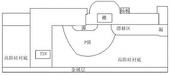
[0010] In LDMOS devices, there is a large current between the source and the ground on the back of the chip. In order to reduce the resistance between the source and the ground, a low-resistance heavily doped P-type silicon substrate is used, and a low-resistance P-type silicon layer is epitaxially grown on it, and LDMOS devices are fabricated in the low-resistance epitaxial layer. The source of LDMOS The pole is connected to the heavily doped P-type substrate through a heavily doped P region.

[0011] LDMOS-based MMIC (Monolithic Microwave Integrated Circuit) needs to integrate passive components such as inductors in the chip. However, the isolation between the low-resistance and heavily dope...


PUM


Abstract

The invention discloses a high-resistance silicon substrate based LDMOS MMIC chip. An LDMOS transistor, an inductor, a capacitor, a resistor, metal connection lines, a graph and a soldering pad are integrated on the chip. The chip is characterized in that a P-type high-resistance silicon substrate without epitaxial layers is used; an LDMOS source electrode in the front of the chip is connected with a metal layer at the back of the chip through a silicon substrate through hole technology. The chip has the advantages that the high-resistance silicon substrate is used, and the DMOS source electrode in the front of the chip is connected with the metal layer at the back of the chip through the silicon substrate through hole technology; by means of the high-resistance silicon substrate, the to-earth parasitic capacitance and consumption of the inductor, the capacitor, the resistor, the metal connection lines, the graph, the soldering pad and the like on the chip is reduced, the LDMOS MMIC performance is improved, and accordingly, metal inter-connection layers are reduced, and the cost is reduced. Meanwhile, the PN-junction capacitance between the LDMOS transistor N-type drain electrode and drift region and the P-type substrate can be reduced, so that the LDMOS transistor output capacitance is reduced, and the LDMOS apparatus bandwidth and power conversion efficiency is improved.

Description

technical field [0001] The invention relates to an LDMOS MMIC chip based on a high-resistance silicon substrate, belonging to the technical field of LDMOS devices. Background technique [0002] In LDMOS devices, there is a large current between the source and the ground on the back of the chip. In order to reduce the resistance between the source and the ground, a low-resistance heavily doped P-type substrate is usually used, and a low-resistance P-type silicon layer is epitaxially grown on it, and an LDMOS device is fabricated in the epitaxial layer. [0003] LDMOS-based MMIC (Monolithic Microwave Integrated Circuit) needs to integrate passive components such as inductors, capacitors, and resistors on the chip. However, the isolation between the low-resistance and heavily doped P-type substrate and the top-layer metal as the ground does not exceed 10um, resulting in a large parasitic capacitance between the ground and the ground, which seriously reduces the Q and self-reso...

Claims


Application Information

Patent Timeline
IPC IPC(8): H01L27/04
Inventor 陈强多新中张复才沈美根任春岭
Owner 江苏博普电子科技有限责任公司
Features
  • R&D
  • Intellectual Property
  • Life Sciences
  • Materials
  • Tech Scout
  • Unparalleled Data Quality
  • Higher Quality Content
  • 60% Fewer Hallucinations
Learn More