Scanning driving circuit used for oxide semiconductor thin film transistor

一种扫描驱动电路、氧化物半导体的技术,应用在半导体器件、电路、电气元件等方向,能够解决GOA驱动电路影响、下拉维持电路部分不能处于较高的电位、功能性不良等问题

Active Publication Date: 2015-03-04
TCL CHINA STAR OPTOELECTRONICS TECH CO LTD
View PDF7 Cites 21 Cited by
  • Summary
  • Abstract
  • Description
  • Claims
  • Application Information

AI Technical Summary

Problems solved by technology

[0006] The purpose of the present invention is to provide a scanning drive circuit for oxide semiconductor thin film transistors, to solve the impact of oxide thin film transistors on the GOA drive circuit, especially the poor functionality caused by leakage problems, and to solve the problem of current oxide semiconductors. The problem that the pull-down maintenance circuit part of the thin-film transistor scan driving circuit cannot be at a higher potential during the non-active period

Method used


Image

  • Scanning driving circuit used for oxide semiconductor thin film transistor
  • Scanning driving circuit used for oxide semiconductor thin film transistor
  • Scanning driving circuit used for oxide semiconductor thin film transistor

Examples


Embodiment Construction

[0038] In order to further illustrate the technical means adopted by the present invention and its effects, the following describes in detail in conjunction with preferred embodiments of the present invention and accompanying drawings.

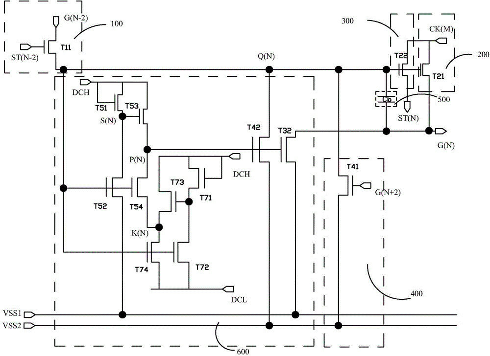
[0039] see Figure 1-5 , is the first embodiment of the scan driving circuit for oxide semiconductor thin film transistors of the present invention. Such as figure 1 As shown, the scan drive circuit for oxide semiconductor thin film transistors is a scan drive circuit for indium gallium zinc oxide (Indium Gallium Zinc Oxide, IGZO) thin film transistors, including a plurality of cascaded GOA units, and N is positive Integer, the Nth stage GOA unit includes a pull-up control part 100 , a pull-up part 200 , a down-pass part 300 , a first pull-down part 400 , a bootstrap capacitor part 500 and a pull-down maintenance circuit part 600 .

[0040] The composition and specific connection of the above parts are as follows:

[0041] The pull-up contr...


PUM


Abstract

The invention provides a scanning driving circuit used for an oxide semiconductor thin film transistor. A pull-down maintaining circuit part (600) of the scanning driving circuit is provided with main inverters and auxiliary inverters which lead in constant-voltage low potential (DCL); and the constant-voltage low potential (DCL) is set to be smaller than second negative potential (VSS2), and the second negative potential (VSS2) is set to be smaller than first negative potential (VSS1). With the scanning driving circuit used for the oxide semiconductor thin film transistor adopted, the electrical properties of the oxide semiconductor thin film transistor will not affect the scanning driving circuit, in particular, poor functional performance caused by electric leakage can be avoided, and the pull-down maintaining circuit part (600) can be normally pulled down in an effect period, and is in high potential in a non-effect period, and a first node (Q (N)) and an output end (G (N)) can be maintained in low potential.

Description

technical field [0001] The invention relates to the field of liquid crystal display, in particular to a scanning driving circuit for an oxide semiconductor thin film transistor. Background technique [0002] GOA (Gate Drive On Array), is to use thin film transistor (thin film transistor, TFT) liquid crystal display array (Array) manufacturing process to make the gate driver on the thin film transistor array substrate, so as to realize the driving method of progressive scanning. [0003] Usually, the GOA circuit is mainly composed of a pull-up part, a pull-up control part, a transfer part, a pull-down part, and a pull-down maintenance circuit part ( Pull-down Holding part) and the rising part (Boost part) which is responsible for raising the potential. The rising part is generally composed of a bootstrap capacitor. [0004] The pull-up part is mainly responsible for outputting the input clock signal (Clock) to the gate of the thin film transistor as a driving signal of the l...

Claims


Application Information

Patent Timeline
Patent Type & Authority Applications(China)
IPC IPC(8): G09G3/36
CPCG09G3/36G09G2300/0408G09G3/3677H01L27/1225H01L29/7869G09G2320/045G09G2320/0214
Inventor 戴超
Owner TCL CHINA STAR OPTOELECTRONICS TECH CO LTD
Why Eureka
Try Eureka