
Clock transfer circuit, video processing system, and semiconductor integrated circuit

A clock conversion and circuit technology, applied in electrical digital data processing, TV system components, standard conversion, etc., can solve problems such as memory control address flaws, and achieve the effect of reducing memory size and preventing quality degradation.

Active Publication Date: 2015-02-25
PANASONIC SEMICON SOLUTIONS CO LTD
View PDF7 Cites 11 Cited by
  • Summary
  • Abstract
  • Description
  • Claims
  • Application Information

AI Technical Summary

Problems solved by technology

[0003] Here, if the interval between the write address and the read address is narrowed sequentially, they will compete with each other, causing a so-called flaw in the memory control address.

Method used


Image

  • Clock transfer circuit, video processing system, and semiconductor integrated circuit
  • Clock transfer circuit, video processing system, and semiconductor integrated circuit
  • Clock transfer circuit, video processing system, and semiconductor integrated circuit

Examples


Embodiment approach 1

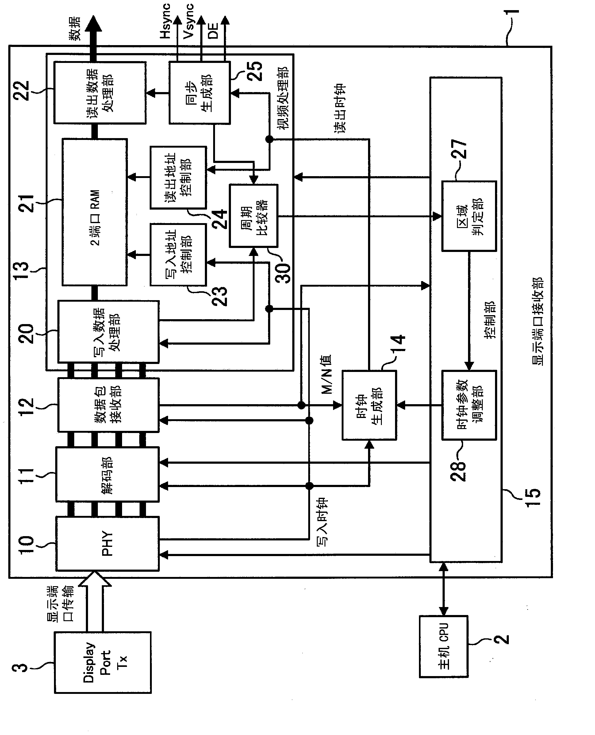
[0036] figure 1 It is a figure which shows the structure of the video processing system of Embodiment 1. in figure 1 In the display port (DisplayPort) receiving unit 1 is controlled by the host (HOST) CPU2, and data is transmitted from the transmitting device 3 through the display port transmission. In the display port receiving unit 1, the data transmitted by the PHY unit 10 is received, and after the decoding (Decode) unit 11 decodes the data, the packet receiving unit 12 receives various data packets. The video processing unit 13 receives the received image data, performs data rearrangement and clock conversion, and outputs video data Data, a horizontal synchronization signal Hsync, a vertical synchronization signal Vsync, and a data valid enable signal DE.

[0037] In the display port, the receiving side generates a read clock based on the write clock based on the clock generation parameters sent from the transmitting side. The clock generation unit 14 receives the clock gen...

Embodiment approach 2

[0064] The configuration and operation of the video processing system in the second embodiment are the same as those in the first embodiment. However, the structure and operation of the period comparator 30 are different.

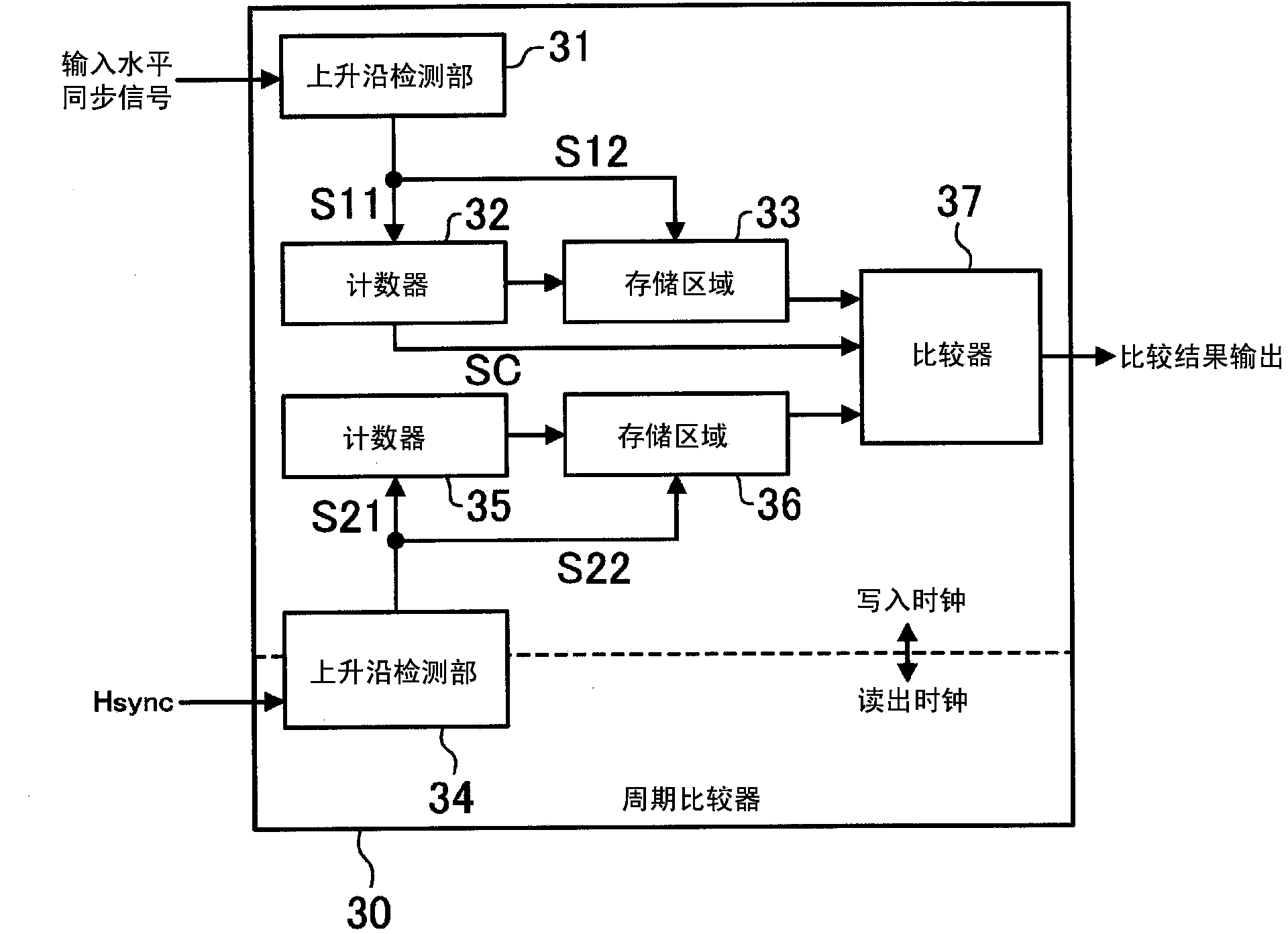
[0065] Picture 9 This is an example of the structure of the period comparator in the second embodiment. Picture 9 The cycle comparator 30 receives the input horizontal synchronization signal and the input vertical synchronization signal from the write data processing unit 20, and receives the Hsync as the output horizontal synchronization signal and the Vsync as the output vertical synchronization signal from the synchronization generation unit 25. The selector 42 as the first selector selects either one of the input horizontal synchronization signal or the input vertical synchronization signal, and supplies it to the rising edge detection unit 31. The selector 43 as the second selector selects and outputs either Hsync or Vsync, and supplies it to the rising...


PUM


Abstract

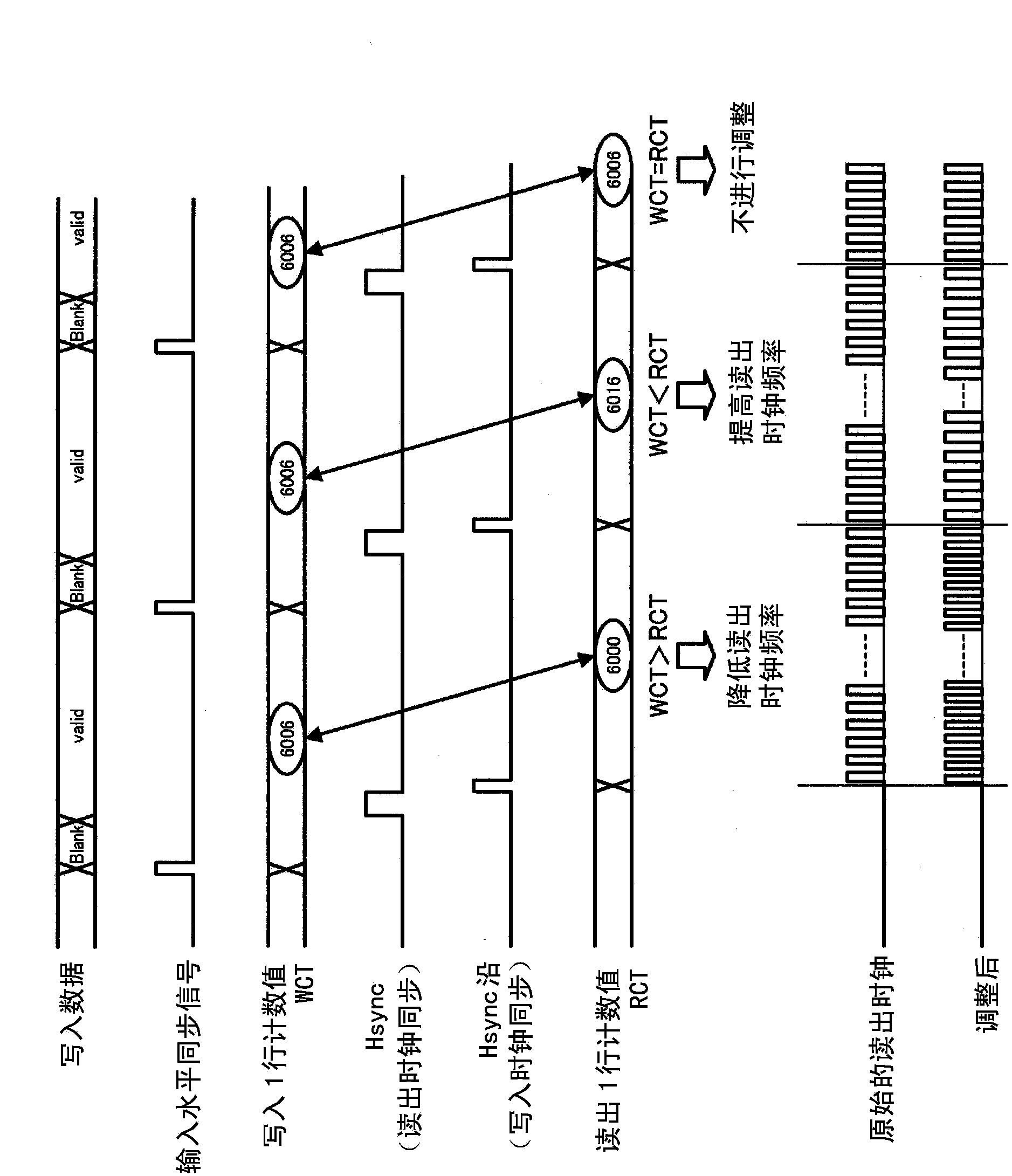
A clock transfer circuit receives input data synchronized with a first clock and outputs the received input data as output data synchronized with a second clock having a different frequency. A write address control unit (23) operates in synchronization with the first clock and supplies a write address to a memory (21). A read address control circuit (24) operates in synchronization with the second clock and supplies a read address to the memory (21). A frequency comparator (30) compares the input data with the output data in the frequency of a predetermined event. Based on this comparison result, clock adjustment units (14, 15) adjust the frequency of the second clock.

Description

Technical field [0001] The present invention relates to a clock conversion circuit that converts data input in synchronization with a clock into clocks of different cycles for output. Background technique [0002] The clock conversion circuit converts the data input in synchronization with the clock into clocks of different cycles for output. The clock conversion circuit uses, for example, a 2-port RAM to control the write address and the read address at an appropriate distance to convert the write data into clocks of different cycles, read them out, and transmit them. [0003] Here, if the interval between the write address and the read address becomes narrower, they will compete with each other, which may cause a so-called memory control address flaw. In the prior art, in order to prevent address contention, the write address and the read address are compared, and the address is reset when the gap between the addresses is narrow and contention is required. [0004] In Patent Docu...

Claims


Application Information

Patent Timeline
IPC IPC(8): H04L7/00
CPCG09G5/006G09G2370/10G09G5/005G09G2340/0435G06F2205/061G06F5/06H04N5/08H04N7/0105H04N21/4305H04N21/43632
Inventor 西尾勇希
Owner PANASONIC SEMICON SOLUTIONS CO LTD
Learn More