Array substrate and display device

一种阵列基板、显示装置的技术,应用在显示装置,阵列基板领域,能够解决开口率损失较大、降低显示装置显示效果和出光效果等问题,达到提高开口率、减小宽度的效果

Active Publication Date: 2015-02-18
TCL CHINA STAR OPTOELECTRONICS TECH CO LTD
View PDF5 Cites 12 Cited by
  • Summary
  • Abstract
  • Description
  • Claims
  • Application Information

AI Technical Summary

Problems solved by technology

However, for a common sub-pixel unit 1 (such as Figure 8 As shown), since the data lines 4 are arranged on the left and right sides of the pixel electrode 9, the area loss value of the opening area of ​​each sub-pixel unit is 2*X1*H1 (H1 is the effective height of the opening area), resulting in a relatively large loss of aperture ratio. Large, reducing the display effect and light output effect of the display device

Method used


Image

  • Array substrate and display device
  • Array substrate and display device
  • Array substrate and display device

Examples


Embodiment 1

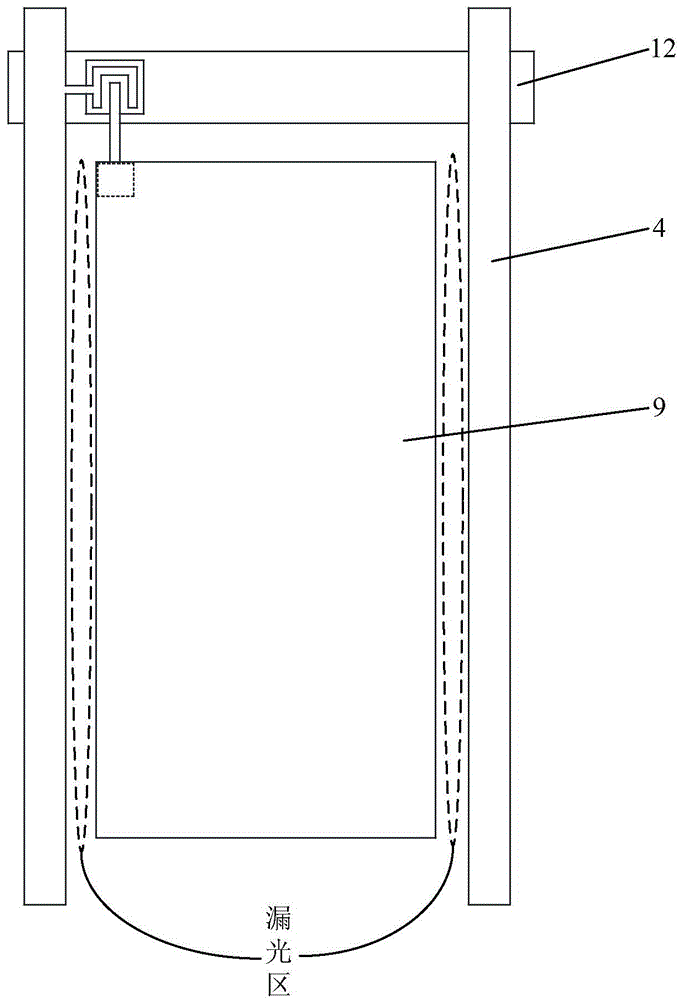
[0038] This embodiment provides an array substrate, such as Figure 9 As shown, the array substrate includes a plurality of sub-pixel unit pairs, wherein each sub-pixel unit pair includes two adjacent sub-pixel units 1 located in a row.

[0039] Specifically, in the same sub-pixel unit pair, the structures of the two sub-pixel units 1 are Figure 9 The dotted line in is the axis of symmetry, which is mirror symmetric. A first common electrode 2 is disposed between the two sub-pixel units 1 , and the first common electrode 2 forms an opaque region.

[0040] Obviously, in the technical solution of the embodiment of the present invention, the opaque region formed by the first common electrode corresponds exactly to the region between two sub-pixel units, which can prevent light leakage between the same sub-pixel unit pair and between two sub-pixel units emergence of the area. Moreover, since both the first common electrode and the sub-pixel units are disposed on the array subs...

Embodiment 2

[0051] This embodiment provides a display device. Specifically, the display device includes the array substrate described in Embodiment 1, and also includes a color filter substrate matched with the array substrate.

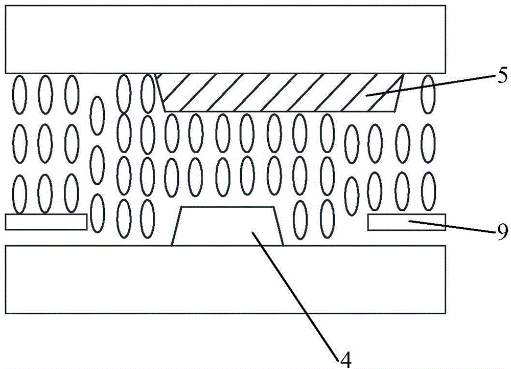
[0052] Specifically, such as Figure 10 As shown, the color filter substrate includes a black matrix 5, and the pattern of the black matrix 5 includes a first area 6 set corresponding to the data line 4 of the array substrate and a second area 6 connected to the first area 6 and set corresponding to the gate line 12. area 7. Additionally, if Figure 11 As shown, a third region 8 disposed corresponding to the first common electrode 2 on the array substrate may also be included. Since no data line 4 is provided between the same sub-pixel unit pair, and the first common electrode 2 between the two sub-pixel unit 1 of the same sub-pixel unit pair can play a role of blocking light, the width of the third region 8 can be different. Restricted.

[0053] which, combi...


PUM


Abstract

The invention discloses an array substrate and a display device and belongs to the field of display technology. By virtue of the array substrate, the occurrence of light leakage area can be avoided under the condition that the aperture opening ratio of the display device is ensured. The array substrate comprises a plurality of sub-pixel unit pairs, wherein each sub-pixel unit pair comprises two sub-pixel units which are arranged in the same row and are adjacent to each other; in the same sub-pixel unit pair, the structures of the two sub-pixel units are arranged in a mirror symmetry manner; a first public electrode is arranged between the two sub-pixel units and is used for forming a light-proof area. The array substrate can be applied to display devices such as liquid crystal display televisions, liquid crystal displays, mobile phones, tablet personal computers and the like.

Description

technical field [0001] The present invention relates to the field of display technology, in particular, to an array substrate and a display device. Background technique [0002] A vertical alignment (Vertical Alignment, VA for short) display device is widely used because of its advantages such as high contrast ratio and large viewing angle. A general VA display device includes an array substrate and a color filter substrate. The array substrate is formed with criss-cross gate lines, data lines, and sub-pixel units surrounded by the gate lines and data lines. The color filter substrate is formed with corresponding sub-pixel unit settings. The color filter and the black matrix corresponding to the grid lines and data lines. The array substrate and the color filter substrate form the liquid crystal panel of the display device by packaging the liquid crystal molecules in the cell. An electric field is formed between the array substrate and the color filter substrate, and the l...

Claims


Application Information

Patent Timeline
Patent Type & Authority Applications(China)
IPC IPC(8): G02F1/1343G02F1/1335
CPCG02F1/133512G02F1/1343G02F1/1362G02F1/133509G02F1/134318G02F1/134345G02F1/133514G02F1/134309G02F1/13439G02F1/136286G02F1/1368H01L27/124
Inventor 郑华
Owner TCL CHINA STAR OPTOELECTRONICS TECH CO LTD
Why Eureka
Try Eureka