Semiconductor process temperature measurement device

A semiconductor and measurement technology, used in semiconductor/solid-state device manufacturing, semiconductor/solid-state device testing/measurement, electrical components, etc., can solve the problem of improper heat treatment temperature control, affecting semiconductor manufacturing yield, and poor temperature monitoring reliability. problems, to achieve a wide and reliable temperature measurement range, long service life, and enhanced reliability.

Inactive Publication Date: 2015-01-21
PREMTEK INT
View PDF9 Cites 0 Cited by
  • Summary
  • Abstract
  • Description
  • Claims
  • Application Information

AI Technical Summary

Problems solved by technology

However, the temperature of the object under test often expands and contracts due to the temperature change during the heat treatment process, and further causes the thermocouple to fall off from the object under test. This not only makes the reliability of temperature monitoring poor, but may even further cause Improper temperature control of heat treatment affects the manufacturing yield of semiconductors

Method used


Image

  • Semiconductor process temperature measurement device
  • Semiconductor process temperature measurement device
  • Semiconductor process temperature measurement device

Examples


Embodiment Construction

[0038] The specific embodiments adopted by the present invention will be further described by the following embodiments and attached drawings.

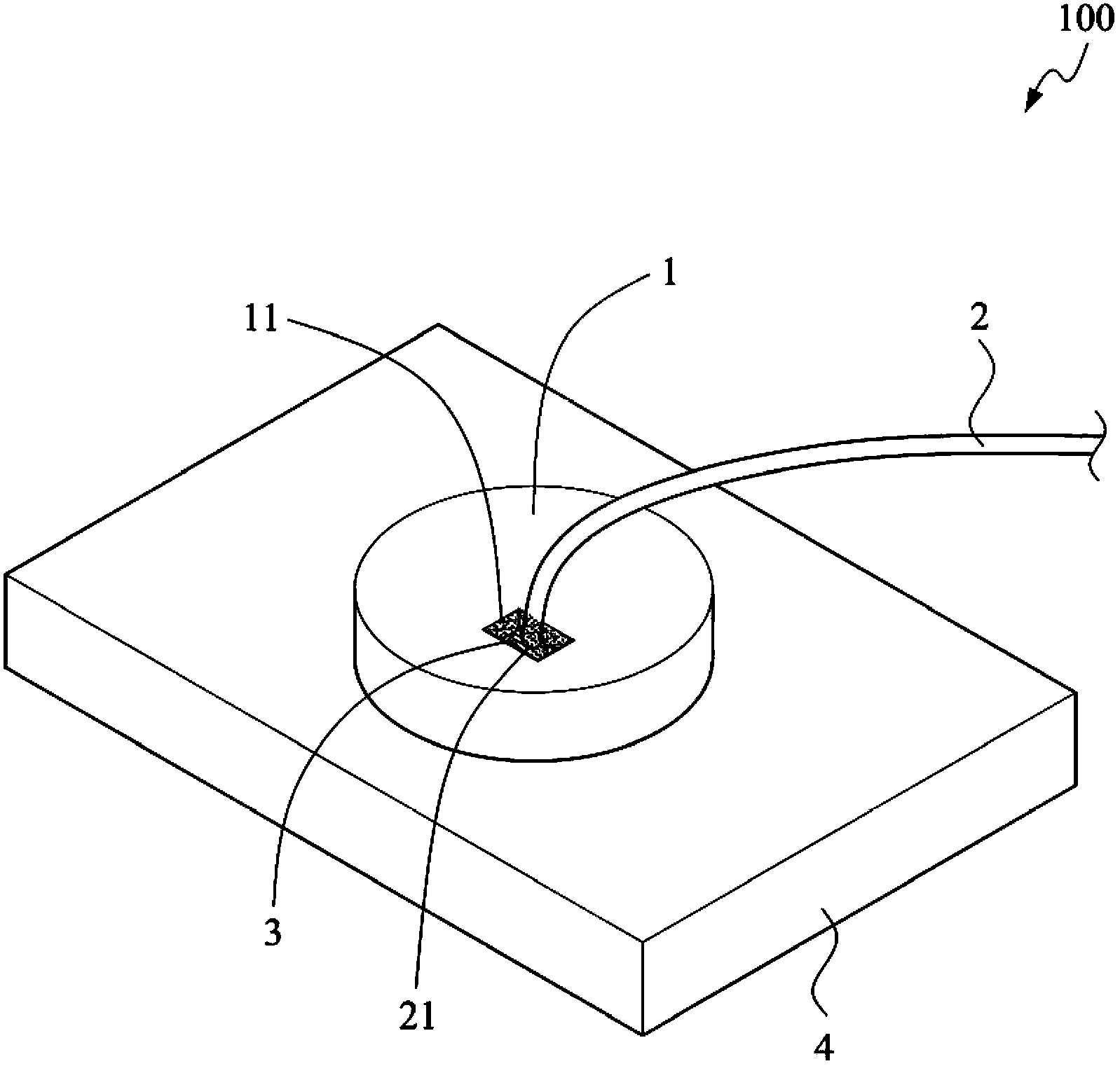
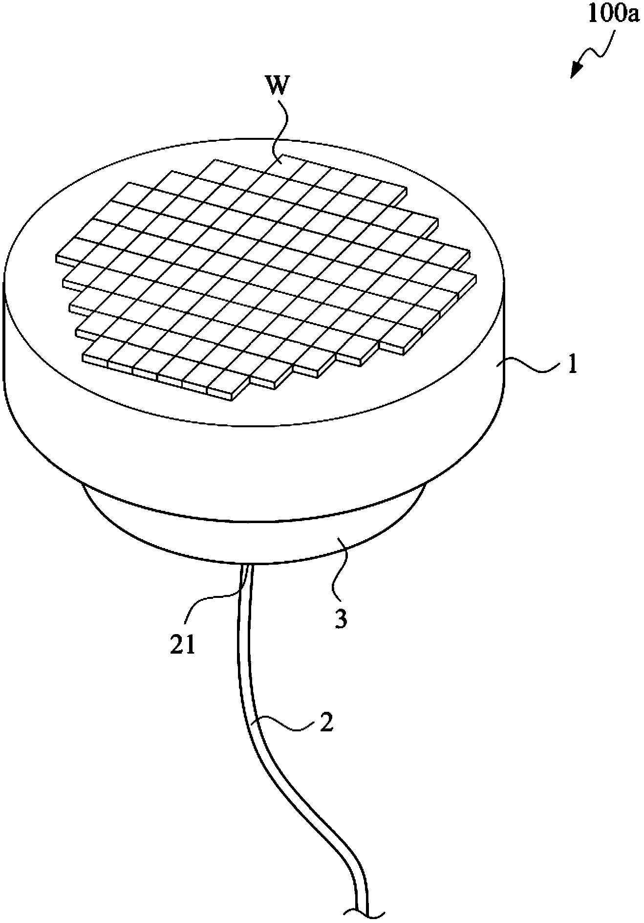
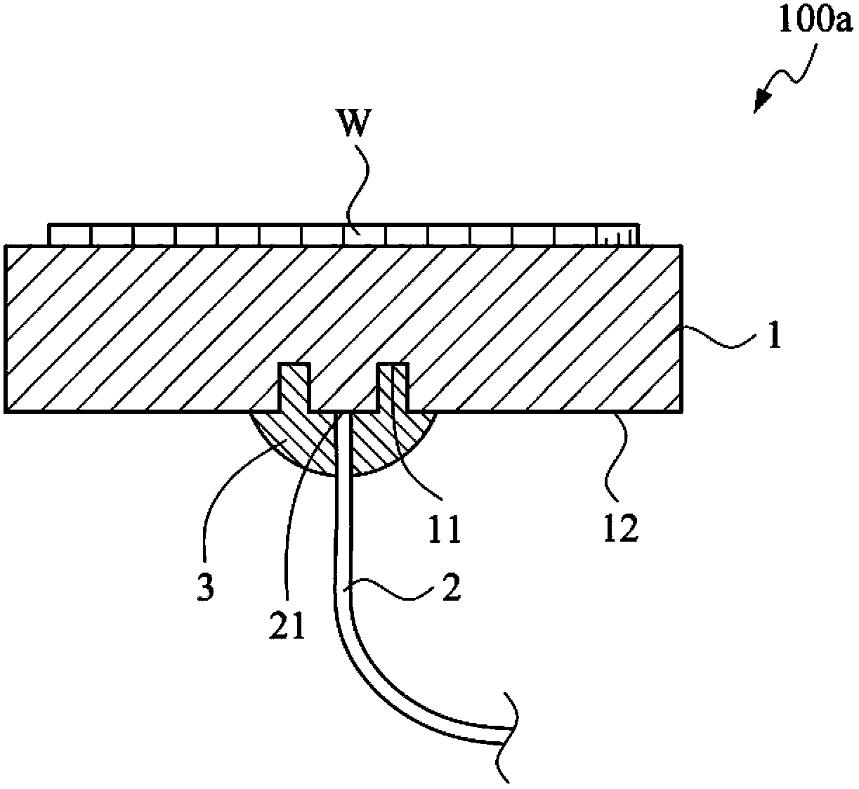
[0039] see figure 1 As shown, a semiconductor manufacturing process temperature measuring device 100 according to an embodiment of the present invention includes a measured body 1 and a temperature measuring member 2. In this embodiment, the measured body 1 is a semiconductor, and an object The body 4 is used to place the body 1 under test. The tested body 1 is formed with a concave portion 11 formed on the upper surface of the tested body 1 .

[0040] A sensing end 21 of the temperature measuring component 2 is connected and thermally contacted with the measured body 1 , and the sensing end 21 is covered by an adhesive object 3 adhered to the concave portion 11 . In this embodiment, the temperature measuring component 2 is a thermocouple (Thermal Coupler), and the adhesive object 3 is a ceramic paste. However, the present inventio...


PUM


Abstract

The invention relates to a semiconductor process temperature measurement device, comprising a measured body and a temperature measuring member. The measured body forms a concave part, and a sensing end of the temperature measuring member is connected and thermally contacted with the measured body. Moreover, the sensing end is wrapped with an adhesion object adhered in the concave part. The measured body is a holding body used for holding a semiconductor and is thermally contacted with the semiconductor for holding the semiconductor; or the measured body is the semiconductor. Therefore, the sensing end of the temperature measuring member is firmly connected to the measured body, thereby enhancing the reliability of semiconductor process temperature monitoring.

Description

technical field [0001] The invention relates to the design of a semiconductor process temperature measuring device, in particular to a highly reliable semiconductor process temperature measuring device. Background technique [0002] Semiconductors can be used as carriers for integrated circuits. The manufacturing process of semiconductors includes many processing methods, including photosensitive agent coating, exposure, development, corrosion, and infiltration, etc., to make components with multi-layer circuits, and to make practical integrated components through inspection and packaging. finished circuit. [0003] The manufacturing process of semiconductors must go through repeated heat treatments, including thermal oxidation process, annealing treatment, AI hot pressing method, heat smoothing treatment, cooling hardening, etc., to gradually manufacture finished products. In order to control the temperature of the heat treatment to achieve the expected manufacturing effe...

Claims


Application Information

Patent Timeline
IPC IPC(8): H01L21/66H01L21/67
CPCH01L21/67248H01L22/10
Inventor 林武郎郑煌玉赖威任王陈右黄政礼陈世敏郭明伦石玉光
Owner PREMTEK INT
Why Eureka
Try Eureka