
A pad structure and its preparation method

A pad and metal layer technology, applied in the field of pad structure and its preparation, can solve the problems of top metal 1 exposure, narrow opening, poor contact between needle and PAD, etc., and achieve the effect of reducing RC) delay

Active Publication Date: 2017-08-04
WUHAN XINXIN SEMICON MFG CO LTD
View PDF3 Cites 0 Cited by
  • Summary
  • Abstract
  • Description
  • Claims
  • Application Information

AI Technical Summary

Problems solved by technology

[0002] With the continuous development of chip testing technology, more and more WAT (Wafer Acceptance Test, wafer acceptance test) and CP (Chip Probing, wafer testing) tests are required in the process development stage, but from the current WAT PAD (welding Disk) and CP PAD design, it is easy to expose the top metal of the PAD after more than 3 times of testing. After oxidation in the air, the direct contact between the needle and the PAD will be poor, which will cause inaccurate test results.
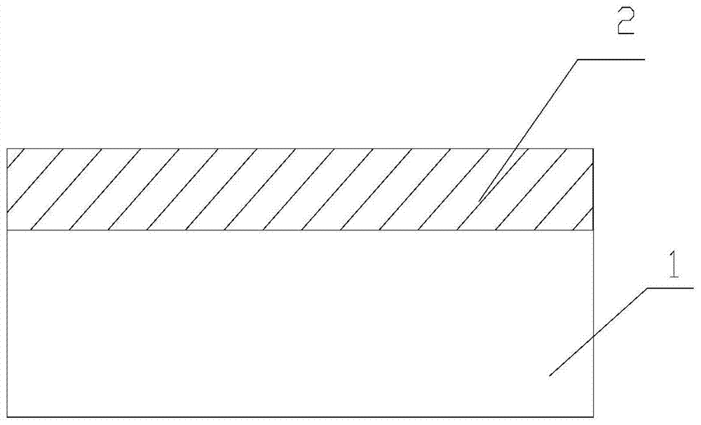
[0003] There are currently two forms of PAD design, such as figure 1 and figure 2 As shown, one is all open, the pad metal 2 is directly connected to the top metal (Top Metal, TM) 1, but after WAT / CP test more than 3 times, the top metal 1 on the PAD will be exposed
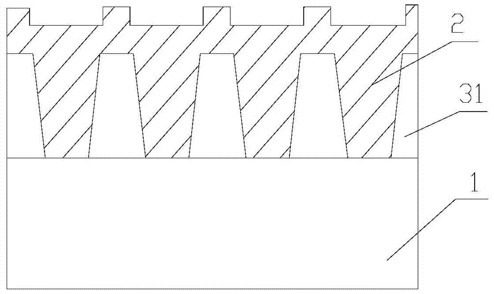
The other is to open a lot of vias / openings (VIA) on the PAD. The pad metal 2 is connected to the top metal 1 through the VIA. When pinning the PAD, the oxide of PAS1 (Passivation layer1, the first passivation layer) ( Oxide, referred to as OX) can prevent the needle from continuing to go down to prevent the PAD from being pierced, but this requires a certain hole-filling ability when the pad metal is deposited, and the side of the VIA (Profile) is not straight, and the opening is relatively narrow. In PAS2 (Passivation layer2, the second passivation layer) etching, the OX on the VIA sidewall (Sidewall) is difficult to etch clean, it is easy to cause PAD bonding (Banding) to fail, and OQA (Outgoing Quality Assurance, factory quality Control) detects PAD residue (Residue), which is undesirable for those skilled in the art

Method used


Image

  • A pad structure and its preparation method
  • A pad structure and its preparation method
  • A pad structure and its preparation method

Examples


Embodiment Construction

[0034] The present invention will be further described below in conjunction with the accompanying drawings and specific embodiments, but not as a limitation of the present invention.

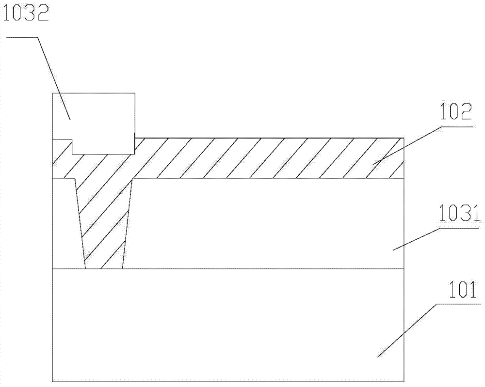
[0035] Such as image 3 As shown, the present invention provides a pad structure, which can be applied in wafer acceptance (WAT) test or wafer test (CP) process, comprising: a top metal layer 101; located on the top metal layer 101 and having The first passivation layer 1031 of the opening; the pad metal layer 102 located above the first passivation layer 1031 and connected to the top metal layer 101 through the opening and the second pad metal layer 102 covering the upper surface of the pad metal layer 102 above the opening Passivation layer 1032; wherein, the opening is located at the edge region of the pad structure, specifically, the pad structure is divided into a middle region and an edge region surrounding the middle region, wherein the middle region is a region for WAT / CP testing, this ...


PUM


Abstract

The present invention relates to the field of semiconductor manufacturing technology, in particular to a pad structure and a preparation method thereof; by forming sufficient openings in the edge region of the pad structure, the connection between the pad metal and the top metal is ensured, and the resistance capacitance (RC ) delay, and open the area without openings when etching the second passivation layer, thereby ensuring that the Banding PAD has no residue and has sufficient flatness, and sufficient test times can be obtained in engineering tests, and the first passivation layer Oxide can be used to block PAD penetration.

Description

technical field [0001] The invention relates to the technical field of semiconductor manufacturing, in particular to a pad structure and a preparation method thereof. Background technique [0002] With the continuous development of chip testing technology, more and more WAT (Wafer Acceptance Test, wafer acceptance test) and CP (Chip Probing, wafer testing) tests are required in the process development stage, but from the current WAT PAD (welding Disk) and CP PAD design, it is easy to expose the top metal of the PAD after more than 3 times of testing. After oxidation in the air, the direct contact between the needle and the PAD will be poor, which will cause inaccurate test results. . [0003] There are currently two forms of PAD design, such as figure 1 and figure 2 As shown, one is all open, the pad metal 2 is directly connected to the top metal (Top Metal, TM) 1, but after WAT / CP test more than 3 times, the top metal 1 on the PAD will be exposed. The other is to open ...

Claims


Application Information

Patent Timeline
Patent Type & Authority Patents(China)
IPC IPC(8): H01L23/488H01L21/60
Inventor 刘念陈俊
Owner WUHAN XINXIN SEMICON MFG CO LTD
Learn More