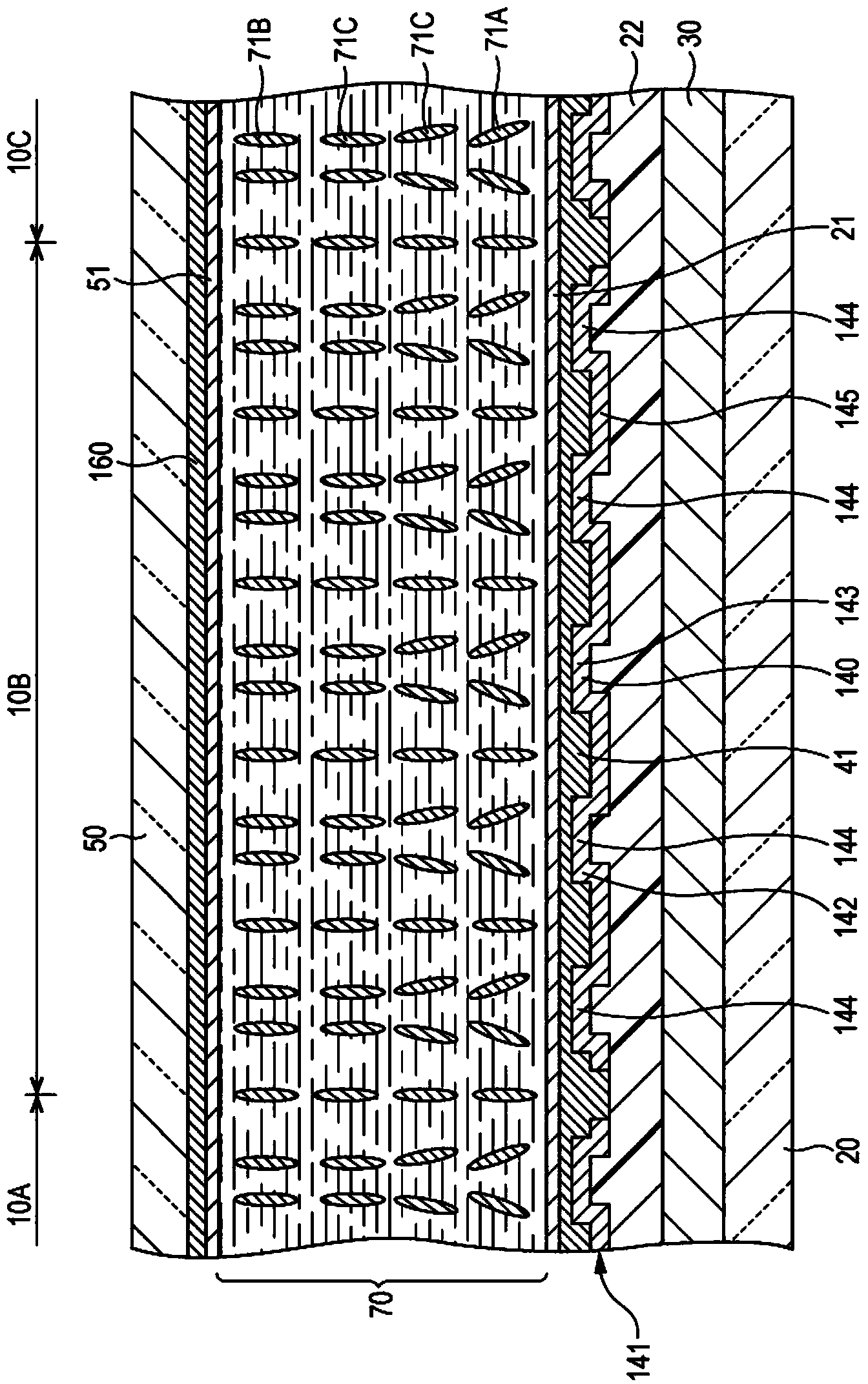
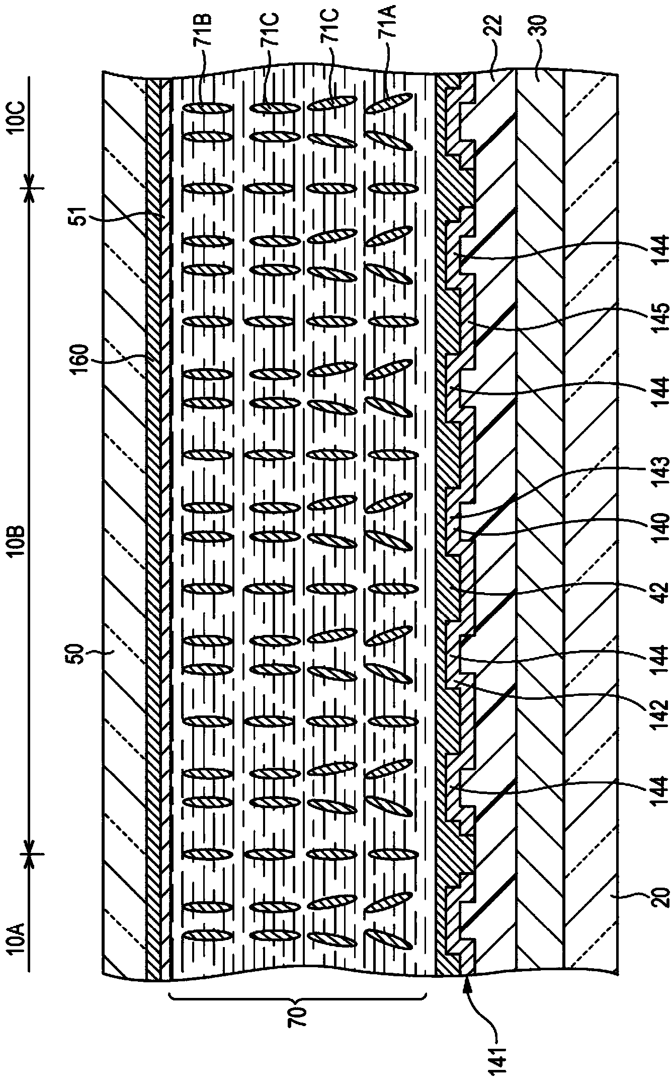
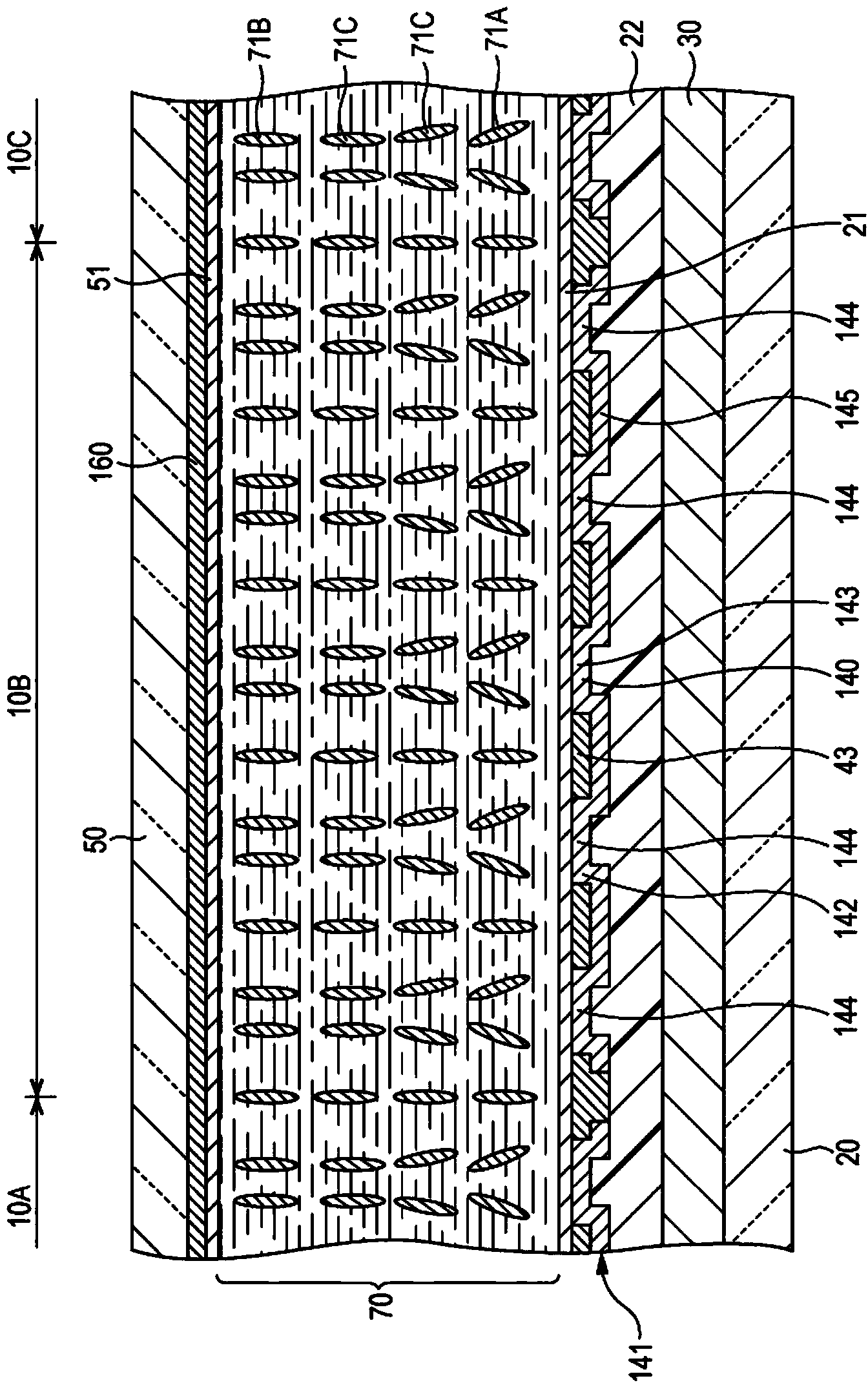
Liquid crystal display device
A liquid crystal display device and liquid crystal layer technology, applied in nonlinear optics, instruments, optics, etc., can solve problems such as differences in light transmittance of display devices, and achieve the effect of uniform orientation state and uniform light transmittance
- Summary
- Abstract
- Description
- Claims
- Application Information
AI Technical Summary
Problems solved by technology
Method used
Image
Examples
Embodiment 5
[0118] 6. Example 5 (Liquid Crystal Display Device According to Embodiment 2A-1 of the Present Disclosure)
[0119] 7. Embodiment 6 (variation of Embodiment 5)
[0120] 8. Embodiment 7 (other modifications of Embodiment 5)
Embodiment 8
[0121] 9. Example 8 (Liquid Crystal Display Device According to Embodiment 2A-2 of the Present Disclosure)
[0122] 10. Embodiment 9 (variation of Embodiment 8)
[0123] 11. Embodiment 10 (other modifications of Embodiment 8)
[0124] 12. Example 11 (the liquid crystal display device according to Embodiment 2B of the present disclosure, including Examples 5 to 10)
[0125] 13. Example 12 (the liquid crystal display device according to Embodiment 2C of the present disclosure, including Embodiment 2A-1 and Embodiment 2-A)
[0126] 14. Example 13 (the liquid crystal display device according to Embodiment 2D of the present disclosure, including the liquid crystal display devices according to Embodiment 2A-2 and Embodiment 2-B)
[0127] 15. Example 14 (liquid crystal display device according to embodiment 3 of the present disclosure, liquid crystal display device according to embodiment 3A of the present disclosure)
[0128] 16. Example 15 (Modification of Example 14, Liquid Cry...
Embodiment 22
[0135] 23. Example 22 (liquid crystal display device according to Embodiment 4A of the present disclosure)
[0136] 24. Embodiment 23 (variation of embodiment 22)
[0137] 25. Embodiment 24 (other variants of Embodiment 22)
[0138] 26. Embodiment 25 (other variants of Embodiment 22)
[0139] 27. Example 26 (Other modifications of Example 22, the liquid crystal display device according to Embodiment 4A-1 of the present disclosure and the liquid crystal display device according to Embodiment 4C of the present disclosure)
[0140] 28. Example 27 (Other modifications of Example 22, the liquid crystal display device according to Embodiment 4A-2 of the present disclosure, the liquid crystal display device according to Embodiment 4C-2 of the present disclosure, and the liquid crystal display device according to Embodiment 4D of the present disclosure)
[0141] 29. Example 28 (other modifications of Example 22, the liquid crystal display device according to the embodiment 4A-3 of t...
PUM
| Property | Measurement | Unit |
|---|---|---|
| Height | aaaaa | aaaaa |
| Width | aaaaa | aaaaa |
| Thickness | aaaaa | aaaaa |
Abstract
Description
Claims
Application Information
 - Generate Ideas
- Intellectual Property
- Life Sciences
- Materials
- Tech Scout
- Unparalleled Data Quality
- Higher Quality Content
- 60% Fewer Hallucinations
Browse by: Latest US Patents, China's latest patents, Technical Efficacy Thesaurus, Application Domain, Technology Topic, Popular Technical Reports.
© 2025 PatSnap. All rights reserved.Legal|Privacy policy|Modern Slavery Act Transparency Statement|Sitemap|About US| Contact US: help@patsnap.com


