Eureka AIR delivers breakthrough ideas for toughest innovation challenges, trusted by R&D personnel around the world.

Large-area optical grating manufacturing method based on ultrashort-pulse laser-induction self-assembly feature

An ultra-short pulse laser and pulsed laser technology, applied in diffraction grating and other directions, can solve the problems of splicing error, time cost of difficult processing technology, exposure wavefront deflection, etc., to achieve high cycle accuracy, saving research and development cycle and cost.

Inactive Publication Date: 2014-12-24
SHANGHAI INST OF OPTICS & FINE MECHANICS CHINESE ACAD OF SCI
View PDF8 Cites 9 Cited by
  • Summary
  • Abstract
  • Description
  • Claims
  • Application Information

AI Technical Summary

Problems solved by technology

[0007] From the current manufacturing method of large-aperture gratings, a single exposure needs to produce large-aperture, high-quality aspheric collimator mirrors. The main problems are difficult processing techniques and unknown time costs; while scanning exposure and exposure splicing method to manufacture large gratings, although the above problems are avoided, but very high requirements are placed on the control of the relative position of the substrate and the exposure beam
Any unstable factors in the exposure and measurement system will introduce stitching errors and affect the diffraction wavefront of the large grating
Although the exposure splicing method has been experimentally verified on a small scale, it still needs to overcome problems such as the deflection of the exposure wavefront, the surface shape of the substrate, exposure aberrations, and seams in order to expand to the production of large-scale gratings.

Method used


Image

  • Large-area optical grating manufacturing method based on ultrashort-pulse laser-induction self-assembly feature
  • Large-area optical grating manufacturing method based on ultrashort-pulse laser-induction self-assembly feature
  • Large-area optical grating manufacturing method based on ultrashort-pulse laser-induction self-assembly feature

Examples


Embodiment

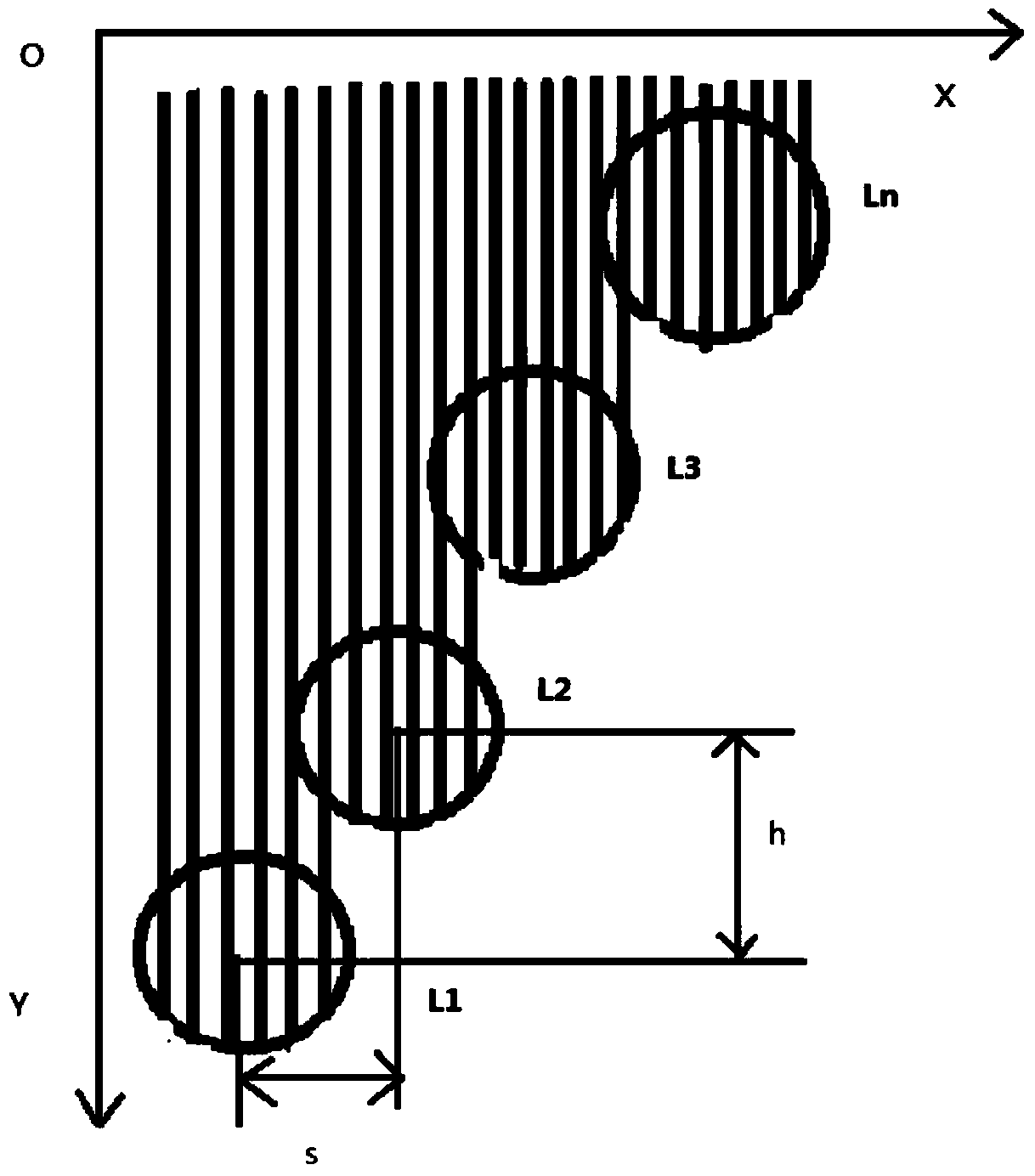
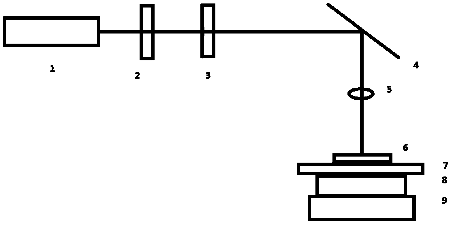
[0073] The technical solution of the present embodiment is as follows:

[0074] A method for fabricating a large-area grating with ultrashort pulse laser-induced self-assembly characteristics, comprising the following steps:

[0075] ①Substrate preparation, selection of functional materials, thin film structure design and thin film preparation;

[0076] ②Pulse laser to process the surface of the material to form a surface grating structure;

[0077] ③In order to speed up the production speed, multiple beams are used to process the grating production materials in parallel;

[0078] ④Transfer of surface grating structure to quartz glass substrate.

[0079] For the selection of functional materials, film structure design and film preparation in the above step ①:

[0080] 1) The selected functional material is metal titanium (Ti);

[0081] 2) The multi-layer structure is as follows: functional film, heat insulation film, reflective film, quartz glass substrate; heat insulation...


PUM


Abstract

The invention provides a large-area optical grating manufacturing method based on an ultrashort-pulse laser-induction self-assembly feature. The method includes the steps of preparing a substrate, processing multiple pulse lasers in a concurrent mode and transferring a surface grating structure to a quartz glass substrate. By means of the method, in the diameter range of laser spot irradiation, grating structures very high in cycle accuracy can be formed spontaneously, and the grating structures can conduct large-area spontaneous growth in a seamless and regular mode along with moving and scanning of laser spots. The method has the advantages of being high in grating manufacturing speed, large in grating area and high in quality and having the feature of laser-induction self-assembly.

Description

technical field [0001] The invention relates to the production of gratings, in particular to a method for producing large-area gratings with ultrashort pulse laser-induced self-assembly characteristics. Background technique [0002] In 1965, M. Birnbaum first reported the phenomenon of grating-like (with obvious stripe features) damage patterns on the surface of semiconductor materials under the action of pulsed ruby ​​laser, which was later called laser-induced periodic surface structure (Laser Induce Periodic Surface Structure). Surface Structure, the English abbreviation is LIPSS). Since then, a large number of experiments have been carried out on a variety of materials such as semiconductors, metals, dielectrics and polymers, and the results have shown that laser-induced grating-like patterns are a universal class of physical phenomena. However, after nearly 50 years of development, there has been no progress in the quality control of grating structures. Therefore, exc...

Claims


Application Information

Patent Timeline
Patent Type & Authority Applications(China)
IPC IPC(8): G02B5/18
Inventor 阮昊卜昌郁
Owner SHANGHAI INST OF OPTICS & FINE MECHANICS CHINESE ACAD OF SCI
Why Eureka
Eureka Blog
Learn More