
Composite circuit board and manufacturing method thereof

A manufacturing method and circuit board technology, which is applied to printed circuit components, structural connection of printed circuits, and assembly of printed circuits with electrical components, can solve the problems of complex manufacturing process of composite circuit boards, and achieve simple and maximum manufacturing methods. The effect of thickness reduction

Active Publication Date: 2017-05-03
CHANGSHU MUTUAL TEK CO LTD
View PDF5 Cites 0 Cited by
  • Summary
  • Abstract
  • Description
  • Claims
  • Application Information

AI Technical Summary

Problems solved by technology

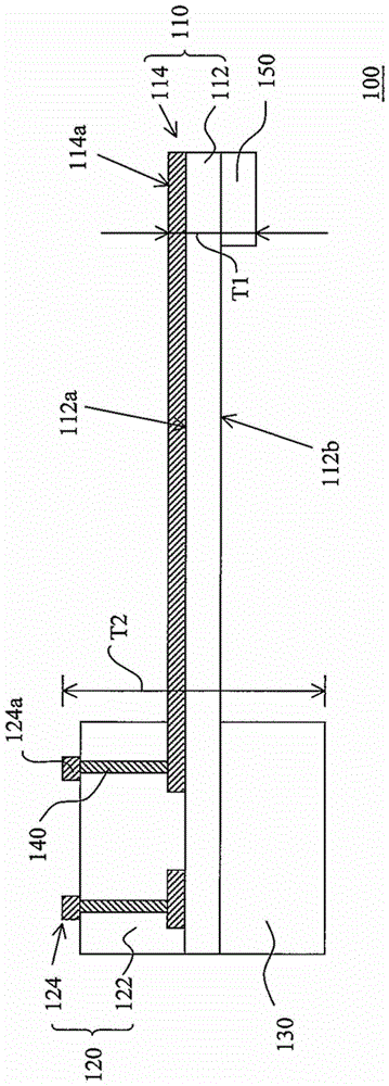
Therefore, the manufacturing process of the existing composite circuit board 100 is relatively complicated.

Method used


Image

  • Composite circuit board and manufacturing method thereof
  • Composite circuit board and manufacturing method thereof
  • Composite circuit board and manufacturing method thereof

Examples


Embodiment Construction

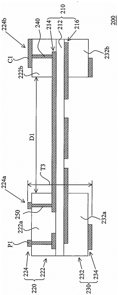
[0048] figure 2 A schematic cross-sectional view of a composite circuit board according to an embodiment of the present invention is shown. Please refer to figure 2 , the composite circuit board 200 of this embodiment includes a flexible circuit board 210 , a plurality of rigid circuit boards 220 and 230 , and a plurality of conductive holes 240 and 250 . The flexible circuit board 210 includes a flexible dielectric layer 212 and two circuit layers 214 and 216 . The circuit layers 214 and 216 are respectively disposed on opposite sides of the flexible dielectric layer 212 . The material of the flexible dielectric layer 212 is, for example, polyimide resin (polyimide, PI) or epoxy resin (epoxy resin).

[0049] The rigid circuit boards 220 and 230 are respectively disposed on opposite sides of the flexible circuit board 210 . The rigid circuit board 220 includes a rigid dielectric layer 222 and a circuit layer 224 . The rigid dielectric layer 222 is disposed on the flexib...


PUM


Abstract

The invention discloses a combined circuit board and a production method thereof. The combined circuit board comprises a flexible circuit board, rigid circuit boards, first conductive vias and second conductive vias. The flexible circuit board comprises a flexible dielectric layer and circuit layers arranged on the flexible dielectric layer. Each rigid circuit board comprises a rigid dielectric layer and a circuit layer comprising a main circuit and an out connection interface circuit. The rigid dielectric layers are arranged on the flexible circuit board. Each rigid dielectric layer comprises a first rigid dielectric portion and a second rigid dielectric portion which are spaced by a distance to enable part of the flexible circuit board to be exposed to the outside. Each main circuit is arranged on the corresponding first rigid dielectric portion. Each out connection interface circuit is arranged on the corresponding second rigid dielectric portion and comprises contacts. The first conductive vias are arranged in the second rigid dielectric portions and electrically connected with the contacts and the circuit layers of the flexible circuit board. The second conductive vias are arranged in the first rigid dielectric portions and electrically connected with the contacts and the circuit layers of the flexible circuit board.

Description

technical field [0001] The invention relates to a circuit board and a manufacturing method thereof, in particular to a composite circuit board and a manufacturing method thereof. Background technique [0002] Generally speaking, an existing circuit board for carrying and electrically connecting a plurality of electronic components is mainly composed of a plurality of circuit layers and a plurality of dielectric layers stacked alternately. These circuit layers are defined by a conductive layer through a patterning process. The dielectric layers are respectively arranged between the adjacent circuit layers for isolating the circuit layers. In addition, the overlapping circuit layers can be electrically connected to each other through conductive vias. In addition, various electronic components (such as active components or passive components) can also be arranged on the surface of the circuit board, and the purpose of electrical signal propagation can be achieved through the ...

Claims


Application Information

Patent Timeline
Patent Type & Authority Patents(China)
IPC IPC(8): H05K1/14H05K1/11H05K3/36
Inventor 赖文钦
Owner CHANGSHU MUTUAL TEK CO LTD
Learn More